

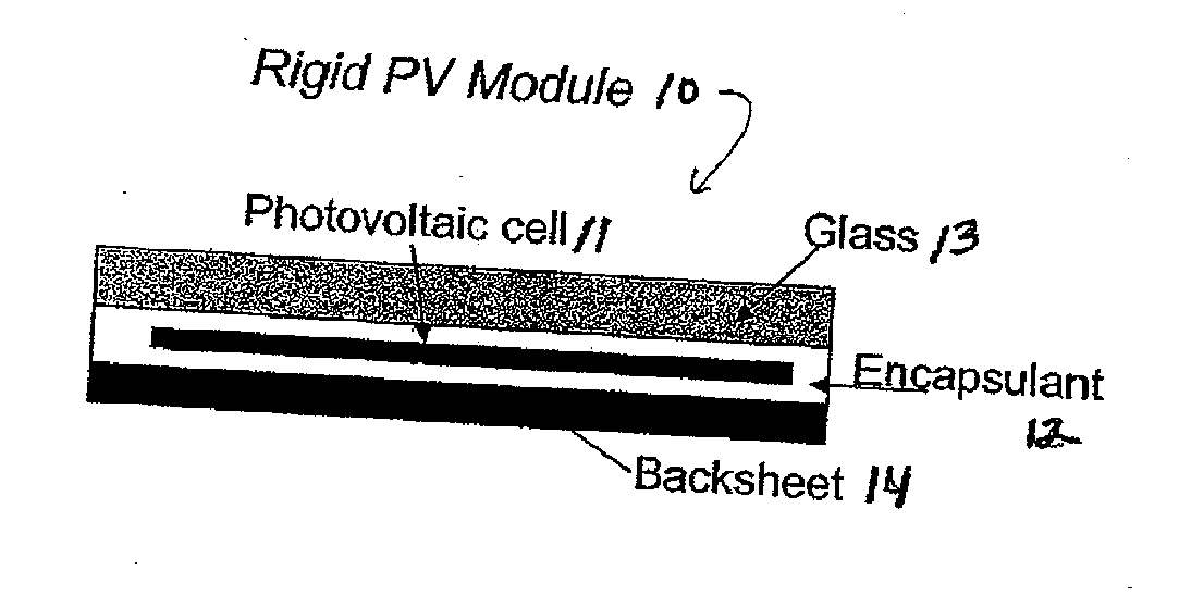
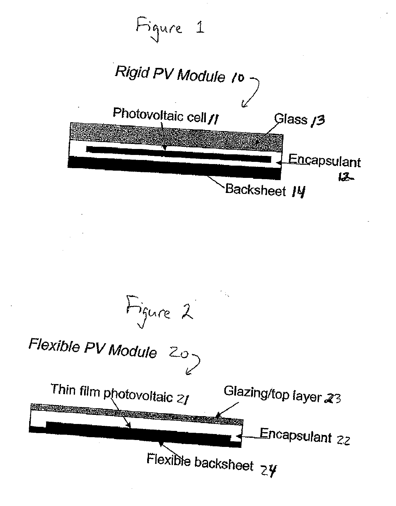
Electronic device module comprising polyolefin copolymer with low unsaturation and optional vinyl silane
a technology of polyolefin copolymer and vinyl silane, which is applied in semiconductor devices, layered products, chemical instruments and processes, etc., can solve the problems of less than ideal pv cell encapsulating film material, greater than 30% loss in power output of solar modules, and eva resins that absorb moisture and other issues, to achieve the effect of good adhesion to glass, faster production rate, and higher processing temperatur
- Summary
- Abstract
- Description
- Claims
- Application Information
AI Technical Summary
Benefits of technology
Problems solved by technology
Method used
Image

Examples
example a
[0145]A monolayer 15 mil thick protective film is made from a blend comprising 80 wt % of example 1 polyethylene, 20 wt % of a maleic anhydride (MAH) modified ethylene / 1-octene copolymer (ENGAGE® 8400 polyethylene grafted at a level of about 1 wt % MAH, and having a post-modified MI of about 1.25 g / 10 min and a density of about 0.87 g / cc), 1.5 wt % of Lupersol® 101, 0.8 wt % of tri-allyl cyanurate, 0.1 wt % of Chimassorb® 944, 0.2 wt % of Naugard® P, and 0.3 wt % of Cyasorb® UV 531. The melt temperature during film formation is kept below about 120 C to avoid premature crosslinking of the film during extrusion. This film is then used to prepare a solar cell module. The film is laminated at a temperature of about 150 C to a superstrate, e.g., a glass cover sheet, and the front surface of a solar cell, and then to the back surface of the solar cell and a backskin material, e.g., another glass cover sheet or any other substrate. The protective film is then subjected to conditions that ...
example b
[0146]The procedure of Example A is repeated except that the blend comprised 90 wt % example 1 and 10 wt % of a maleic anhydride (MAH) modified ethylene / 1-octene (ENGAGE® 8400 polyethylene grafted at a level of about 1 wt % MAH, and having a post-modified MI of about 1.25 g / 10 min and a density of about 0.87 g / cc), and the melt temperature during film formation was kept below about 120° C. to avoid premature crosslinking of the film during extrusion.
example c
[0147]The procedure of Example A is repeated except that the blend comprised 97 wt % example 3 and 3 wt % of vinyl silane (no maleic anhydride modified ENGAGE® 8400 polyethylene), and the melt temperature during film formation was kept below about 120° C. to avoid premature crosslinking of the film during extrusion.
Formulations and Processing Procedures:
[0148]Step 1: Use ZSK-30 extruder with Adhere Screw to compound resin and additive package with or without Amplify.
[0149]Step 2: Dry the material from Step 2 for 4 hours at 100 F maximum (use W&C canister dryers).
[0150]Step 3: With material hot from dryer, add melted DiCup+Silane+TAC, tumble blend for 15 min and let soak for 4 hours.
TABLE 1FormulationSample No.1EXAMPLE 194.74-Hydroxy-TEMPO0.05Cyasorb UV 5310.3Chimassorb 944 LD0.1Tinuvin 622 LD0.1Naugard P0.2Additives below added via soaking stepDicup-R Peroxide2Gamma-methacrylo-propyl-trimethoxysilane1.75(Dow Corning Z-6030)Sartomer SR-507 Tri-Allyl Cyanurate (TAC)0.8Total100
Test Met...
PUM
| Property | Measurement | Unit |
|---|---|---|
| temperature | aaaaa | aaaaa |
| UV-wavelengths | aaaaa | aaaaa |
| wavelength | aaaaa | aaaaa |
Abstract
Description
Claims
Application Information