Method and apparatus for removing a reversibly mounted device wafer from a carrier substrate

a technology of carrier substrate and device wafer, which is applied in the direction of grinding feeders, manufacturing tools, lapping machines, etc., can solve the problems of high thermal and mechanical stress on the device wafer, the inability to form backside electrical contacts that connect with the front-side circuitry, and the thinned device wafers that have been less than 100 microns thinned to less than 60 microns

Active Publication Date: 2011-12-22
BREWER SCI
View PDF11 Cites 137 Cited by
  • Summary
  • Abstract
  • Description
  • Claims
  • Application Information

AI Technical Summary

Benefits of technology

[0024]The present invention is also broadly concerned with a method of forming a temporary wafer bonding structure. The method comprises providing a first substrate having front and back surfaces; forming a bonding layer on the front surface of the first substrate; providing a second substrate having front and back surfaces, the front surface having a surface-modifie...

Problems solved by technology

Without thinning, it would be nearly impossible to form backside electrical contacts that connect with front-side circuitry by passing the connections through the wafer.
Device wafers that have been thinned to less than 100 microns, and especially those thinned to less than 60 microns, are extremely fragile and must be supported over their full dimensions to prevent cracking and breakage.
Various wafer wands and chucks have been developed for transferring ultrathin device wafers, but the problem still exists of how to support the wafers during backgrinding and TSV-formation processes that include steps such as chemical-mechanical polishing (CMP), lithography, etching, deposition, annealing, and cleaning, because these steps impose high thermal and mechanical stresses on the device wafer as it is being thinned or after thinning.
(1) Chemical—The bonded wafer stack is immersed in, or sprayed with, a solvent or chemical agent to dissolve or decompose the polymeric adhesive.
(2) Photodecomposition—The bonded wafer stack is irradiated with a light source through a transparent carrier to photodecompose the adhesive boundary layer that is adjacent to the carrier. The carrier can then be separated from the stack, and the balance of the polymeric adhesive is removed from the device wafer while it is held on a chuck.
(3) Thermomechanical—The bonded wafer stack is heated above the softening temperature of the polymeric adhesive, and the device wafer is then slid or pulled away from the carrier while being supported with a full-wafer holding chuck.
(4) Thermodecomposition—The bonded wafer stack is heated above the decomposition temperature of the polymeric adhesive, causing it to volatilize and lose adhesion to th...

Method used


Image

  • Method and apparatus for removing a reversibly mounted device wafer from a carrier substrate
  • Method and apparatus for removing a reversibly mounted device wafer from a carrier substrate
  • Method and apparatus for removing a reversibly mounted device wafer from a carrier substrate

Examples


example 1

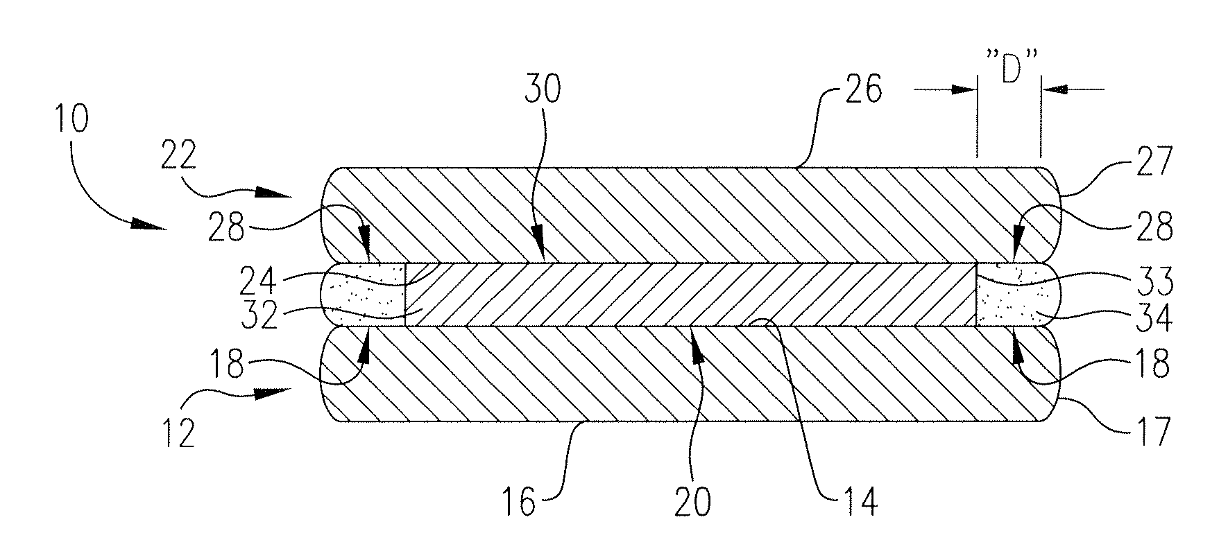
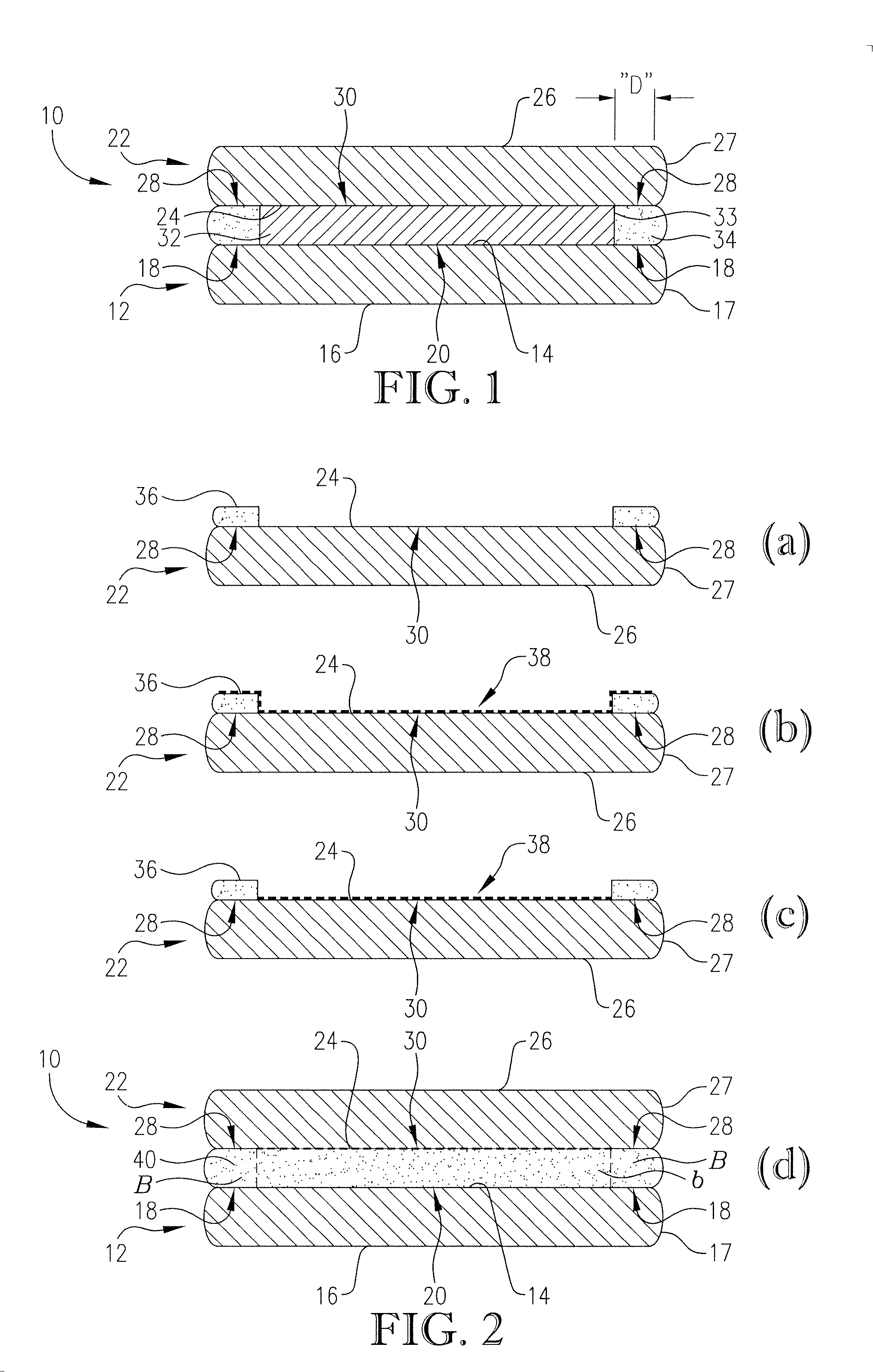
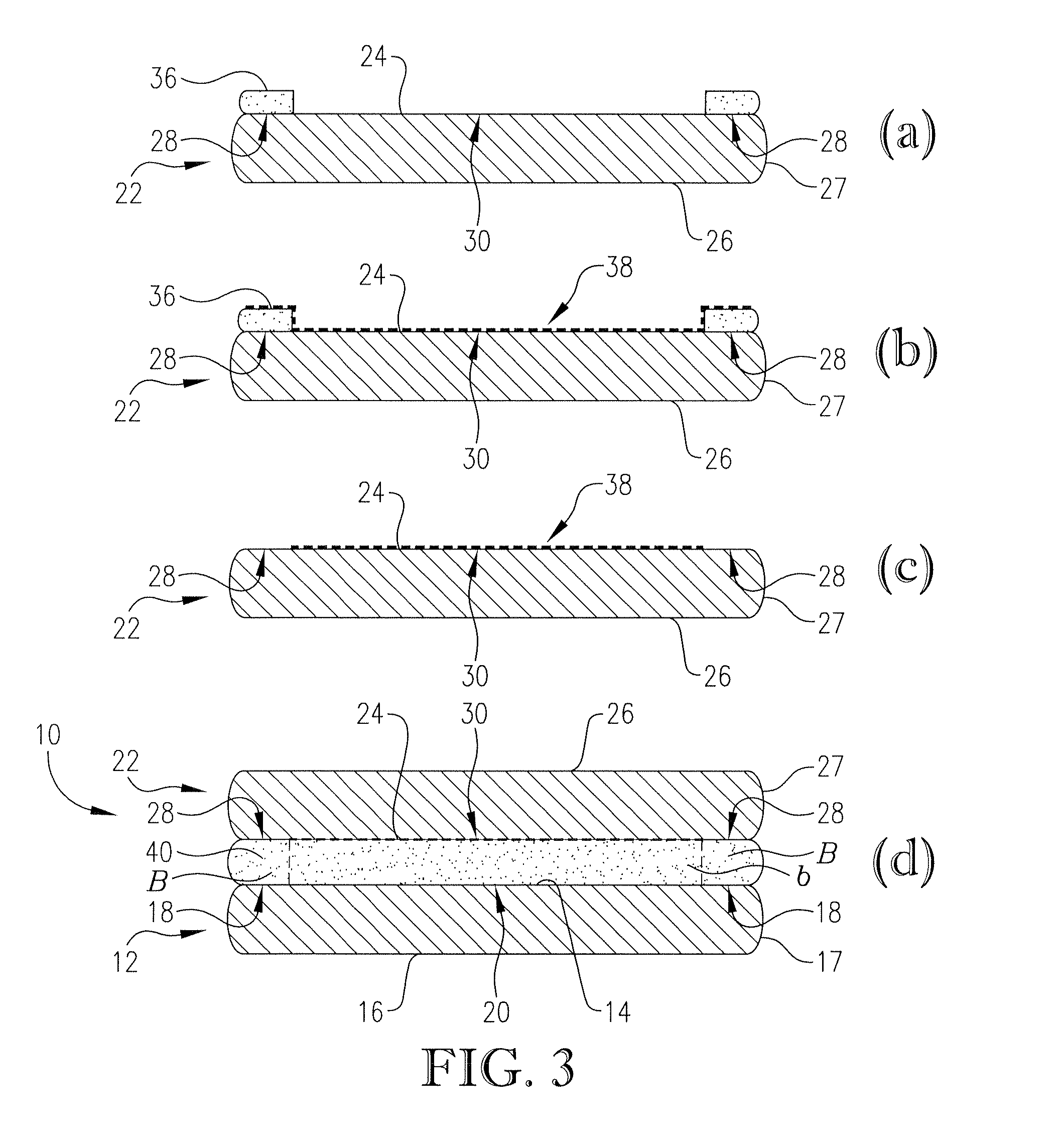
Separation of Edge-Bonded Wafers Having Modified Center Surface Using Hand-Operated Peeler with Removal of Bonding Material from the Outer Edge

[0100]In this procedure, a wafer stack is prepared according to a method of the invention and then separated using a hand-operated peel separator. Prior to adhering the two wafers together, the center contact surface of one wafer is chemically modified using a fluorinated silane solution to create an adhesive strength differential across the wafer surface. A bonding material (WaferBOND® HT10.10, available from Brewer Science, Inc., Rolla, Mo.) was dispensed onto the surface of a 200-mm silicon wafer (wafer 1) at the outer edge to form a very thin coating around the peripheral region of the wafer surface that was about 2.5 mm wide by approximately 0.5 μm thick. A surface-modifying composition was formed by diluting a fluorinated silane ((heptadecafluoro-1,1,2,2-tetrahydradecyl) trichlorosilane; Gelest Inc., Morrisville, Pa.) to a 1% solution u...

example 2

Separation of Adhered Wafer Stack Using Hand-Operated Peel Separator

[0104]In this procedure, a wafer stack is prepared according to another method of the invention and then separated using a hand-operated peel separator. Prior to adhering the two wafers together, the center surface of one silicon wafer is chemically modified using a fluorinated silane solution to create an adhesive strength differential across the wafer surface. To modify the center surface of the wafer, the edge of the wafer was first masked using a coating of an epoxy-based photoresist (SU-8 2002, Microchem, Newton, Mass.). The photoresist composition was dispensed onto the outer edge surface of a 200-mm silicon wafer (wafer 1) to coat a peripheral ring-shaped section of the wafer surface that was about 2.5 mm wide.

[0105]Next, a fluorinated silane ((hepta-decafluoro-1,1,2,2-tetrahydradecyl)trichlorosilane; Gelest, Morrisville, Pa.) was diluted to a 1% solution using FC-40 solvent (perfluoro-alkyl compound with pri...

example 3

Hand-Operated Peel Separator Used to Separate Wafer Stack with Center Contact Surface Coated with Release Material

[0108]In this procedure, a wafer stack is prepared according to another method of the invention and then again separated using a hand-operated peel separator. Prior to adhering the two wafers together, the center surface of one wafer is coated with a release material to create an adhesive strength differential across the wafer surface-center layer interface. First, a negative epoxy-based photoresist (sold under the name SU-8 2010; obtained from MicroChem) was spin coated onto the entire surface of a 200-mm glass wafer (wafer 1), followed by baking at 110° C. for 2 minutes to effect solvent removal. A Teflon® AF solution (Teflon® AF2400 in FC-40; obtained from DuPont) was then spin coated over the photoresist layer to create a nonstick layer. Next, FC-40 solvent was dispensed onto the surface of the wafer at the outer edge to remove about a 1-3 mm wide section of the Tefl...


PUM

PropertyMeasurementUnit
Thicknessaaaaaaaaaa
Thicknessaaaaaaaaaa
Angleaaaaaaaaaa

Abstract

New demounting methods and apparatuses for separating temporarily, permanently, or semi-permanently bonded substrates and articles formed from those methods and apparatuses are provided. The methods comprise demounting a device wafer from a carrier wafer or substrate that have only been strongly bonded at their outer perimeters. The edge bonds are chemically, mechanically, acoustically, or thermally softened, dissolved, or disrupted to allow the wafers to be easily separated with very low forces and at or near room temperature at the appropriate stage in the fabrication process. A clamp for facilitating separation of the bonded substrates is also provided.

Description

BACKGROUND OF THE INVENTION[0001]1. Field of the Invention[0002]The present invention is broadly concerned with novel temporary wafer debonding methods and apparatuses that can remove a device wafer from a carrier substrate after wafer thinning and other backside processing.[0003]2. Description of the Prior Art[0004]Integrated circuits, power semiconductors, light-emitting diodes, photonic circuits, microelectromechanical systems (MEMS), embedded passive arrays, packaging interposers, and a host of other silicon- and compound semiconductor-based microdevices are produced collectively in arrays on wafer substrates ranging from 1-12 inches in diameter. The devices are then separated into individual devices or dies that are packaged to allow practical interfacing with the macroscopic environment, for example, by interconnection with a printed wiring board. It has become increasingly popular to construct the device package on or around the die while it is still part of the wafer array. ...

Claims


Application Information

Patent Timeline
IPC IPC(8): B26D5/42B26D3/28
CPCH01L21/187H01L21/67092H01L21/6835H01L21/68721H01L21/02002H01L21/67011B24B37/345B24B41/005H01L21/3212H01L2221/68318H01L2221/6834H01L2221/68381H01L2221/68386Y10T156/1978Y10T156/1989Y10T156/1168Y10S156/93Y10S156/941
Inventor MCCUTCHEON, JEREMY W.BROWN, ROBERT D.
Owner BREWER SCI
Why Eureka
Try Eureka