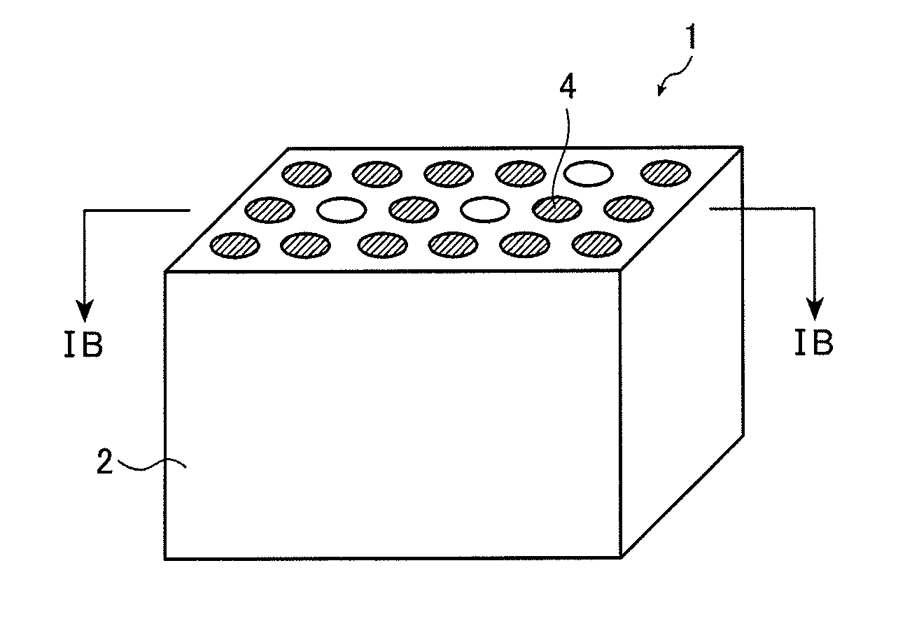
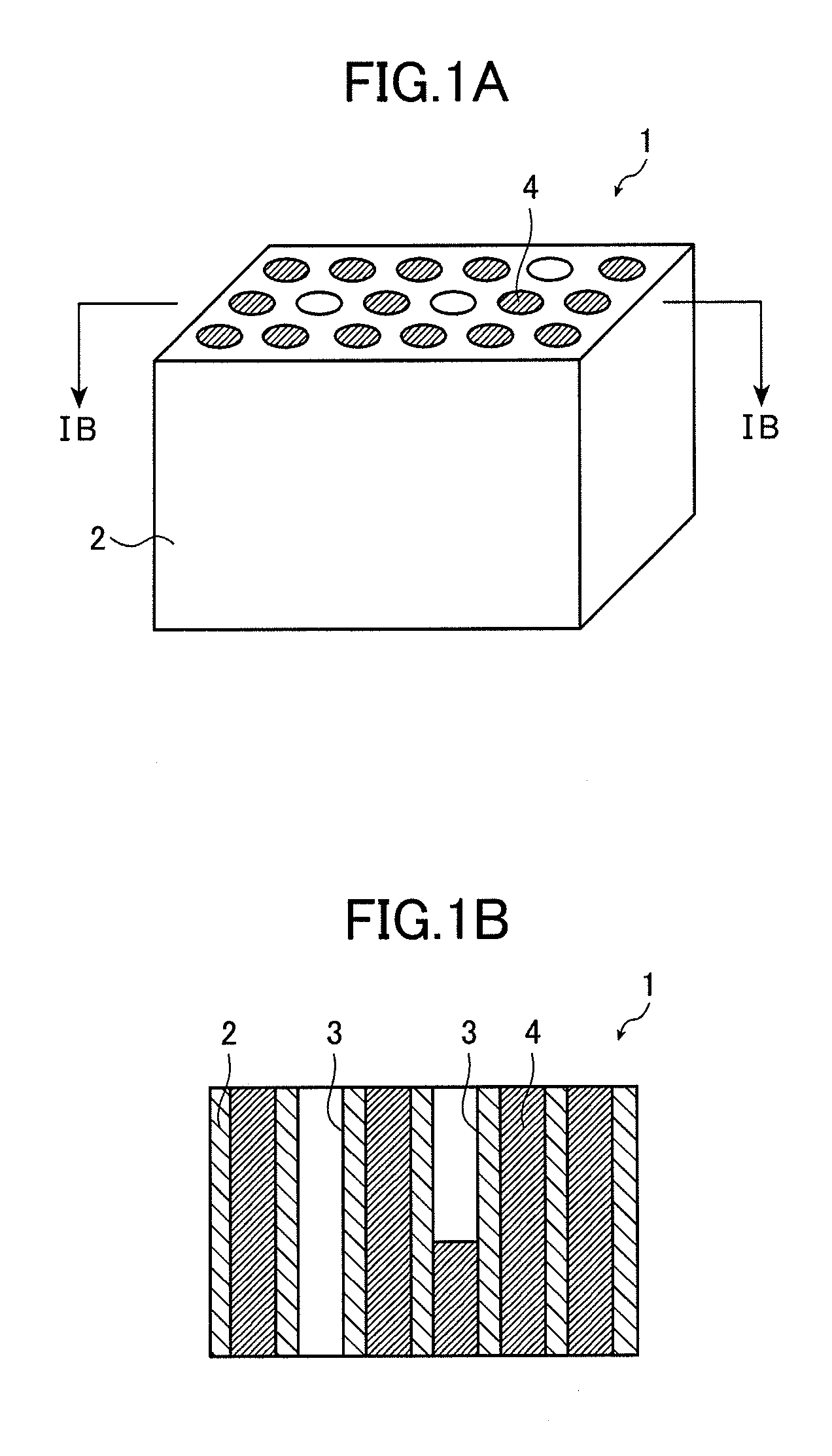
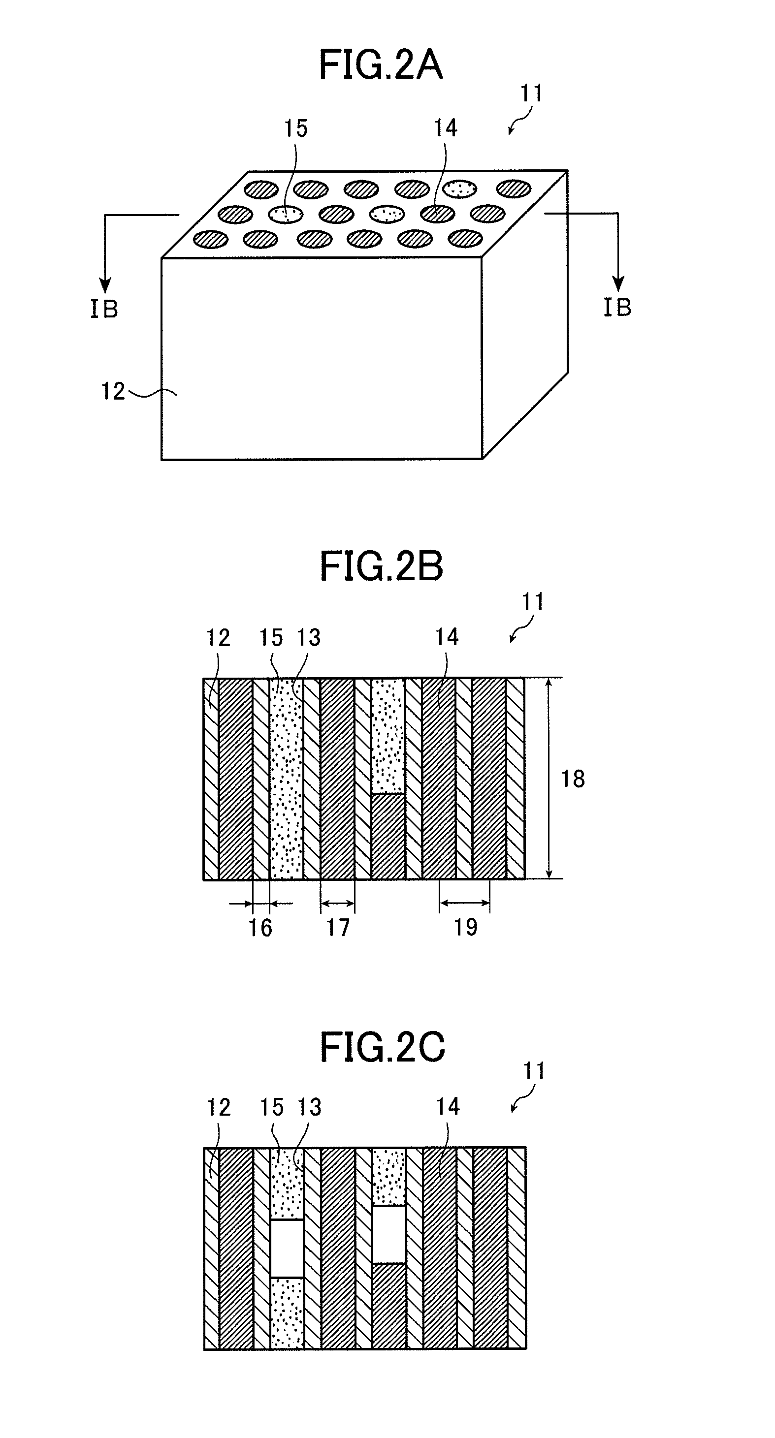
Microstructure and microstructure production method
Inactive Publication Date: 2011-12-22
FUJIFILM CORP
View PDF4 Cites 13 Cited by
Summary
Abstract
Description
Claims
Application Information
AI Technical Summary
This helps you quickly interpret patents by identifying the three key elements:
Problems solved by technology
Method used
Benefits of technology
[0020]As will be described below, the present invention can provide a mic
Problems solved by technology
In particular, given significant miniaturization of electronic connection members such as semiconductors, conventional method
Method used
Image
Click on the blue label to locate the original text in one second.
Reading with bidirectional positioning of images and text.
[0110]A high-purity aluminum substrate (purity 99.99 mass %, thickness 0.4 mm, produced by Sumitomo Light Metal Industries, Ltd.) was cut to an area of 10 cm×10 cm for anodization and allowed to undergo an elctrolytic polishing treatment with a voltage of 25 V at a liquid temperature of 65° C. and at a liquid flow rate of 3.0 m / min using an electrolytic polishing solution having the following composition.
[0111]A carbon electrode was used as cathode, and a GP0110-30R unit (Takasago, Ltd.) was used as power supply. In addition, the flow rate of the electrolytic solution was measured using the FLM22-10PCW vortex flow monitor manufactured by As One Corporation.
(Electrolytic Polishing Solution Composition)
[0112]
85 mass % Phosphoric acid (Wako Pure Chemical660mLIndustries, Ltd.)Pure water160mLSulfuric acid150mLEthylene glycol30mL
(B) Anodizing Treatment
[0113]After electrolytic polishing, the aluminum substrate was subjected...
Example
Comparative Examples 1 and 2
[0147]Comparative examples 1 and 2 of a 100-μm thick microstructure are produced respectively by the same methods as in Examples 1 and 7 except that the sealing treatment was not effected.
Example
[0148]A 100-μm thick microstructure was produced by the same method as in Example 1 except that the sealing treatment A was replaced by the following sealing treatment (polymer filling treatment) (G) described in JP 2010-33753 A.
Sealing Treatment (G)
[0149]First, the metal filled microstructure was immersed in an immersion liquid having the following composition, followed by 1-minute drying at 140° C.
[0150]Then, 850-nm IR was applied to form a 5-μm thick polymer layer in the through-holes.
[0151]This treatment was thereafter repeated 19 times.
[0152]Composition of Immersion Liquid
Radical polymerizable monomer (represented by general0.4120 gformula C below)Photothermal conversion agent (represented by general0.0259 gformula D below)Radical generator (represented by general formula E below)0.0975 g1-Methoxy-2-propanol3.5800 gMethanol1.6900 g[Chemical Formula 1]
[0153]The sealing rates of Examples 1 to 8 and Comparative Example 3 of microstructure produced as described above were measured ...
PUM
Property
Measurement
Unit
Length
aaaaa
aaaaa
Length
aaaaa
aaaaa
Fraction
aaaaa
aaaaa
Abstract
A microstructure enabling provision of an anisotropic conductive member capable of reducing wiring defects and a method of producing such microstructure. The microstructure includes through-holes formed in an insulating matrix and filled with a metal and an insulating substance. The through-holes have a density of 1×10⁶ to 1×10¹⁰ holes/mm2, a mean opening diameter of 10 nm to 5000 nm, and a mean depth of 10 μm to 1000 μm. The sealing ratio of the through-holes as attained by the metal alone is 80% or more, and the sealing ratio of the through-holes as attained by the metal and the insulating substance is 99% or more. The insulating substance is at least one kind selected from the group consisting of aluminum hydroxide, silicon dioxide, metal alkoxide, lithium chloride, titanium oxide, magnesium oxide, tantalum oxide, niobium oxide, and zirconium oxide.
Description
BACKGROUND OF THE INVENTION[0001]The present invention relates to a microstructure and a microstructure production method.[0002]Metal-filled microstructures (devices) where a metal is filled in micropores formed in a matrix are one of the fields in nano-technologies that have been attracting attention in recent years.[0003]An anisotropic conductive member, when inserted between an electronic component such as a semiconductor device and a circuit board, then merely subjected to pressure, is able to provide an electrical connection between the electronic component and the circuit board. Accordingly, such members are widely used, for example, as electric connection members for electronic components such as semiconductor devices and as inspection connectors used to inspect the functions of such components.[0004]In particular, given significant miniaturization of electronic connection members such as semiconductors, conventional methods such as wire bonding whereby circuit boards are dir...
Claims
Application Information
Patent Timeline
Application Date:The date an application was filed.
Publication Date:The date a patent or application was officially published.
First Publication Date:The earliest publication date of a patent with the same application number.
Issue Date:Publication date of the patent grant document.
PCT Entry Date:The Entry date of PCT National Phase.
Estimated Expiry Date:The statutory expiry date of a patent right according to the Patent Law, and it is the longest term of protection that the patent right can achieve without the termination of the patent right due to other reasons(Term extension factor has been taken into account ).
Invalid Date:Actual expiry date is based on effective date or publication date of legal transaction data of invalid patent.