Method for manufacturing a sputtering target structure

a target structure and sputtering technology, applied in the direction of diaphragms, metal-working apparatus, metallic material coating processes, etc., can solve the problems of no more reuse, sputtering target may crack, and large deformation, and achieve stable sputtering, low cost, and the effect of reducing the linear expansion coefficien

Inactive Publication Date: 2012-04-26
PLANSEE SE
View PDF6 Cites 2 Cited by
  • Summary
  • Abstract
  • Description
  • Claims
  • Application Information

AI Technical Summary

Benefits of technology

[0036]In the sputtering target structure of the invention, the difference in the linear expansion coefficient between the sputtering target and the backing plate is small; and therefore, even at high temperatures, the structure does not warp and the sputtering target and the backing plate therein do not peel from each other, and the structure enables stable sputtering. In addition, the sputtering target structure of the invention is inexpensive and can be used repeatedly many times, and its economical advantages are great.

Problems solved by technology

However, its linear expansion coefficient is 17×10−6 / K and is large, and this is problematic in that its deformation is great owing to its elongation in repeated use and, after used a few times, it could no more be reused.
The deformation produces some problems in that the sputtering target may crack, the soldering material may fuse and the soldered part may peel.
Therefore, the requirement for the sputtering target structure free from the above-mentioned problems is great.
These methods are to attain the effect through modification of the constitution of the thin solder material layer between the sputtering target and the backing plate, and they could hardly attain the intended effect.
In these methods, in addition, the minus effect of thermal conductivity depression owing to the disposition of various materials between the sputtering target and the backing plate cannot be bypassed.
Further, the use of indium is problematic in point of its cost.
However, these materials have poor machinability, and are hardly applicable to large-sized products for FPD for which, in particular, the thermal expansion difference between the sputtering target and the backing plate is especially problematic.
However, its thermal conductivity is extremely low and this is unfavorable to a structure of a sputtering target and a backing plate equipped with a cooling mechanism.

Method used


Image

  • Method for manufacturing a sputtering target structure
  • Method for manufacturing a sputtering target structure
  • Method for manufacturing a sputtering target structure

Examples


example 1

[0084]This is described with reference to the drawings.

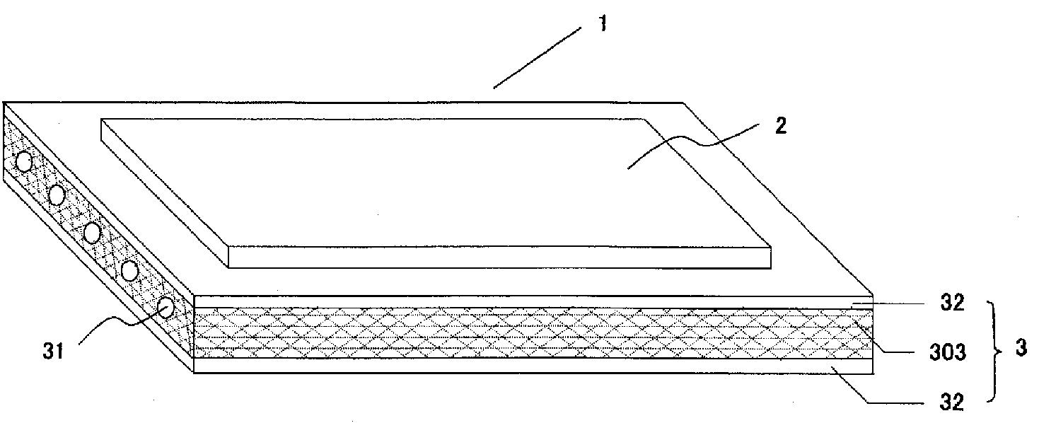
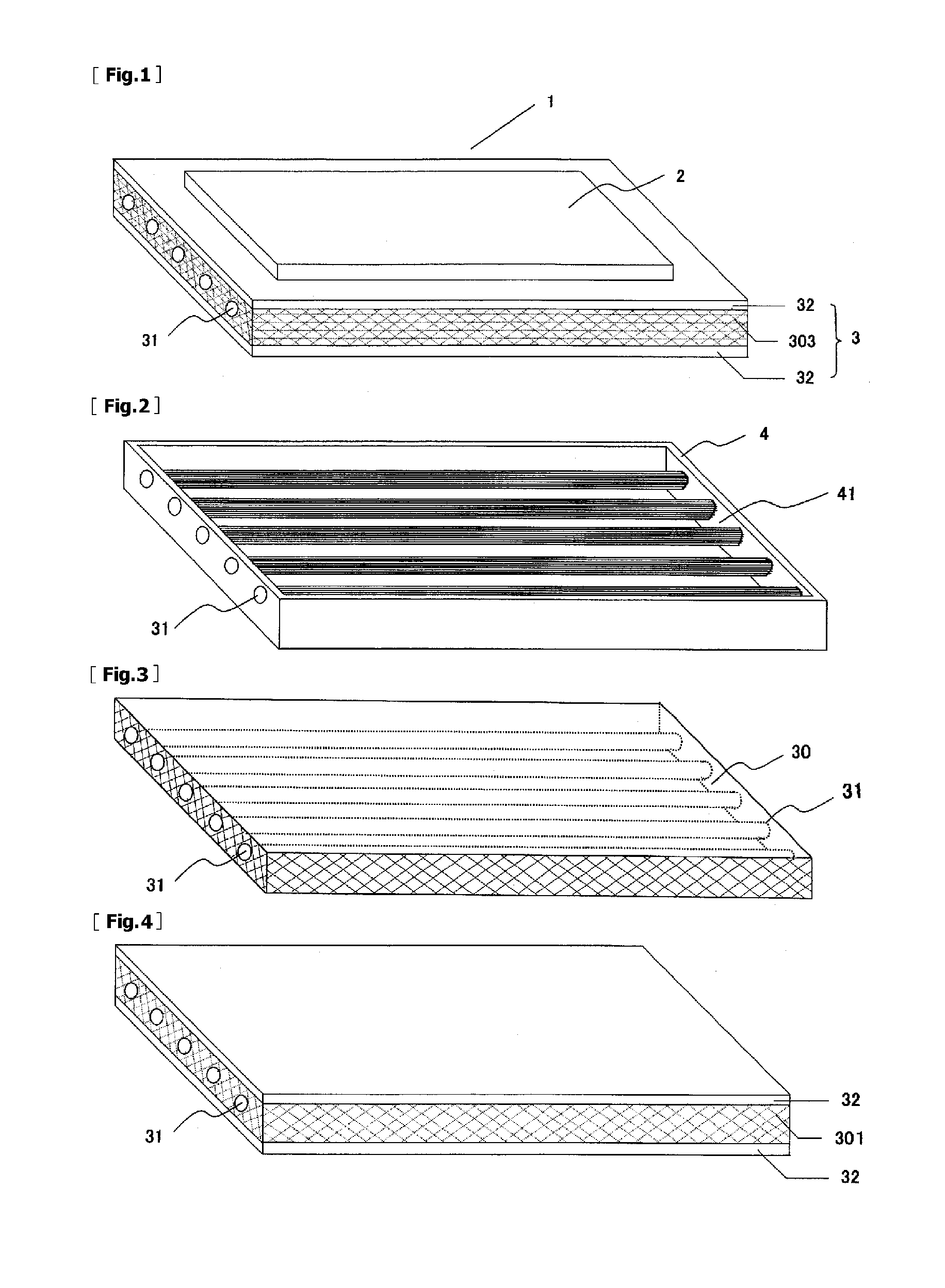
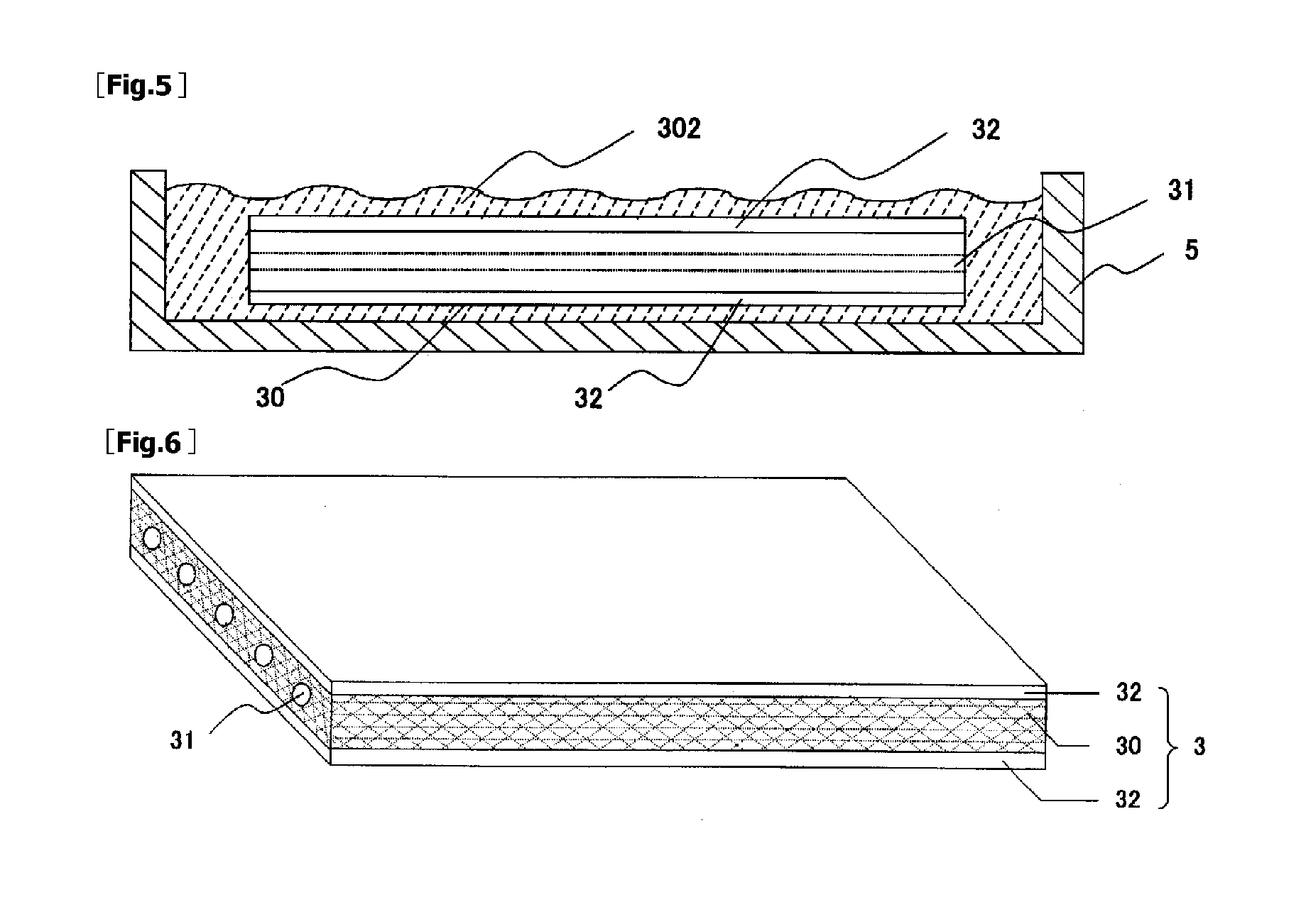
[0085]Five stainless steel pipes 31 (outer diameter 15 mm, pipe wall thickness 1 mm) were aligned in an iron chamber 4 having a length of 2,000 mm a width of 400 mm and a depth of 40 mm, at regular intervals in the cross direction of the chamber (the distance between the side of the chamber and the outermost pipe in the cross direction was 30 mm), in such a manner that the distance from the bottom surface or the top surface of the chamber to the pipe could be the same (FIG. 2). The space 41 was filled with a reinforcing material, or that is, carbon fibers 301 having a diameter of 8 μm and a length of 10 mm so that the volume percentage of the carbon fibers in the space 41 could be 30%. Next, 5% by weight of silica sol was cast into it, dried at 100° C., then fired in nitrogen at 700° C., and thereafter the iron chamber 4 was removed to obtain a carbon fiber shaped article 30 with the stainless steel pipes 31 built therein (FIG. ...

example 2

[0092]In the same manner as in Example 1, five copper pipes (their cross section is oval, having a major diameter of 25 mm, a minor diameter of 8 mm and a pipe wall thickness of 1.5 mm) were aligned in the same iron chamber as that used in Example 1. A mixed silicon carbide powder (#120 / #400=3 / 1) was formed into a slurry with 3% silica sol in such a manner that the powder content could be 500 g / liter. The slurry was cast into the space of the iron chamber. This was dried at 120° C., and then fired in air at 600° C., and a silicon carbide shaped article with copper pipes built therein was thus obtained.

[0093]In the same manner as in Example 1, a copper plate was disposed on both faces of the shaped article. Also similarly, an aluminium melt was cast into the chamber and solidified under high pressure, and a backing plate was thus obtained, comprising a composite material of aluminium and silicon carbide, having copper pipes built therein, and having copper plates disposed on both sur...


PUM

PropertyMeasurementUnit
thicknessaaaaaaaaaa
thicknessaaaaaaaaaa
thicknessaaaaaaaaaa

Abstract

To provide a sputtering target structure which has good machinability and thermal conductivity and has good wettability with soldering materials, which is inexpensive and can be used repeatedly for a long period of time, and which is free from problems of cracking and peeling of the sputtering target therein, a sputtering target structure is formed by bonding a sputtering target and a backing plate. The backing plate is formed of a material that has the difference in the linear expansion coefficient between it and the sputtering target material of at most 2×10⁻⁶ / K, and a copper plate having a thickness of from 0.3 to 1.5 mm is disposed on at lest one face of the backing plate.

Description

[0001]This application is a division of application Ser. No. 12 / 159,739 filed on Jun. 30, 2008; which is the 35 U.S.C. 371 national stage of International application PCT / JP2006 / 326070 filed on Dec. 27, 2006; which claimed priority to Japan application 2005-376811 filed Dec. 28, 2005, respectively. The entire contents of each of the above-identified applications are hereby incorporated by reference.TECHNICAL FIELD[0002]The present invention relates to a sputtering target structure for use in a sputtering step in production of a thin film for hard coating or decorative coating of flat panel displays (hereinafter referred to as “FPD”) such as liquid-crystal displays, plasma displays, etc.BACKGROUND ART[0003]Thin film formation through sputtering comprises introducing a rare gas such as argon into a vacuum chamber, applying a negative voltage to the sputtering target in the chamber to cause glow discharge therein, making the thus-formed plasma cations collide with the sputtering target...

Claims


Application Information

Patent Timeline
Patent Type & Authority Applications(United States)
IPC IPC(8): B22D19/04
CPCB22F7/062C23C14/3407C22C49/06C22C47/08C23C14/34
Inventor KUNIYA, TSUTOMUSUZUKI, NOBUYUKITERASHI, AKIRA
Owner PLANSEE SE
Why Eureka
Try Eureka