Photovoltaic device structure and method

a photovoltaic device and photovoltaic technology, applied in the direction of semiconductor/solid-state device manufacturing, semiconductor devices, electrical devices, etc., can solve the problems of unsatisfactory performance of devices using laser doping in conjunction with anti-reflection coatings, unsatisfactory mixing of dopants, and unwanted ablation of doped silicon, so as to reduce the generation of defects

Active Publication Date: 2012-05-24
NEWSOUTH INNOVATIONS PTY LTD
View PDF4 Cites 24 Cited by
  • Summary
  • Abstract
  • Description
  • Claims
  • Application Information

AI Technical Summary

Benefits of technology

[0039]The proposed multilayer anti-reflection coating may be used with a range of surface structures including textured surfaces and the density of defects generated due to thermal expansion mismatch can be dependent upon this surface geometry. Never-the-less, regardless of the surface geometry, the multilayer anti-reflection coating can be applied so as to significantly reduce the generation of defects during thermal processes.

Problems solved by technology

To date, despite more than a decade of research and problem solving, devices using laser doping in conjunction with an anti-reflection coating, have not achieved their expected performance due to defects, junction recombination or shunting arising from the laser doping process.
In particular, defects adjacent to the melted regions resulting from the thermal expansion mismatch between the silicon and the overlying antireflection coating (ARC), inadequate mixing of the dopants incorporated into the molten silicon and unwanted ablation of the doped silicon are significant problems contributing to the poor electrical performance of devices using laser doping of localised areas beneath the metal contacts.
Most commercially manufactured solar cells use a SLARC as it is too complex and expensive to use a DLARC for the small additional benefits in performance.
Two problems that can result from using an ARC are: firstly, an ARC may make it difficult to passivate the semiconductor surface onto which it is deposited, therefore leading to increased recombination and device dark saturation current; and secondly, many potential ARC materials will have different thermal expansion coefficients to the semiconductor material onto which it is deposited, leading to stressing of the semiconductor surface with possible corresponding defect generation during treatment at elevated temperature.
However to date, a suitable solution does not appear to have been proposed for simultaneously achieving good ARC properties while simultaneously providing thermal expansion mismatch correction for the ARC and passivating the semiconductor material and surface.

Method used


Image

  • Photovoltaic device structure and method
  • Photovoltaic device structure and method
  • Photovoltaic device structure and method

Examples


Embodiment Construction

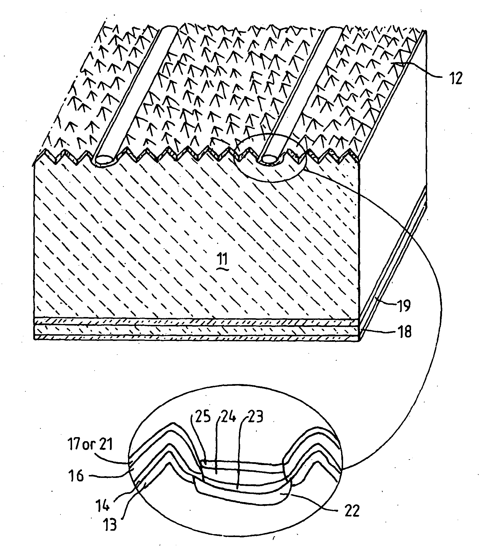
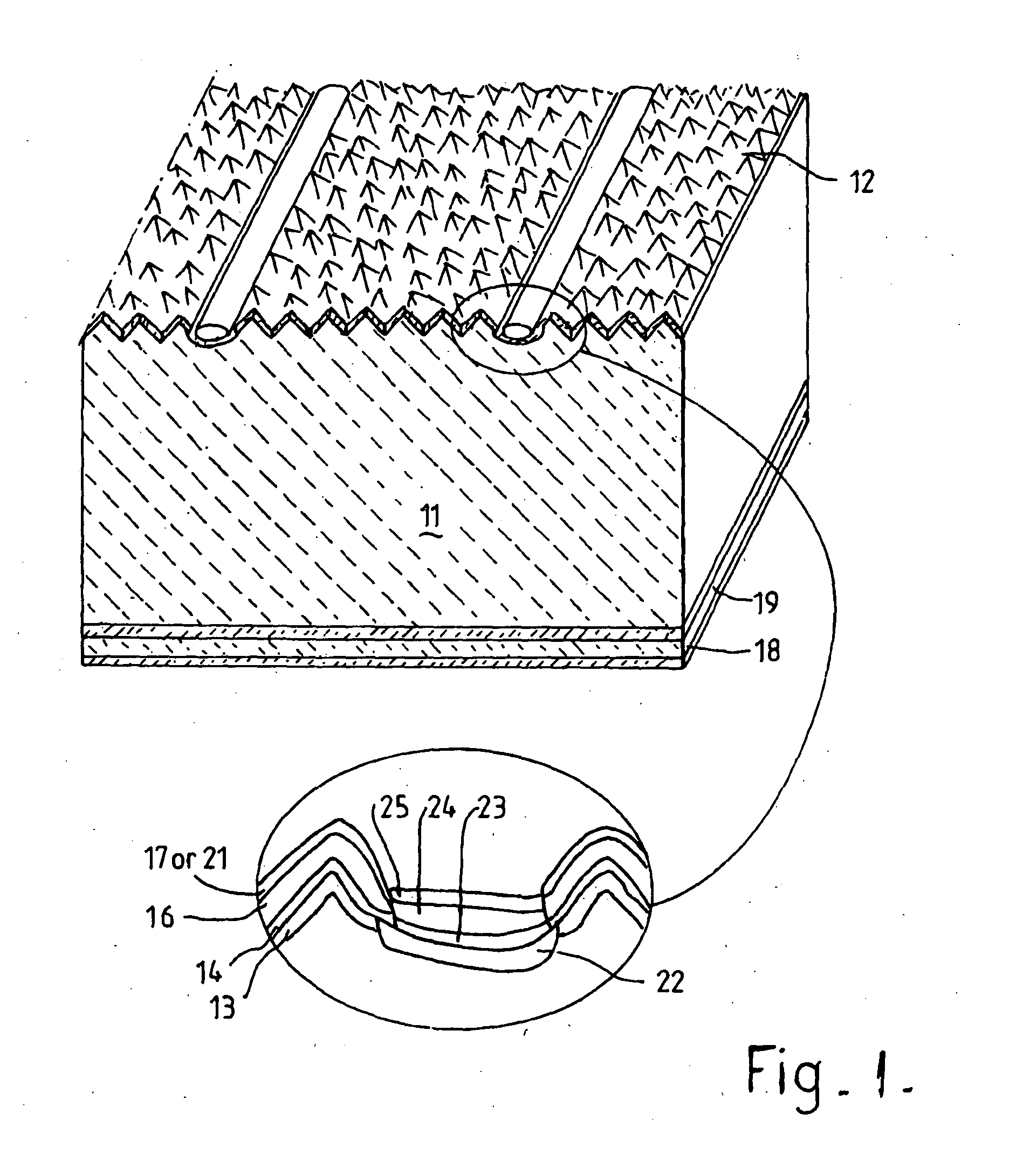
[0111]The application of the multi-layer ARC to multicrystalline silicon wafers has demonstrated efficiencies in the vicinity of 17% using standard commercial grade p-type multicrystalline silicon wafers. An example of a suitable fabrication sequence is as follows:

1. Isotropic texturing 12 of the front (or light receiving) surface of the p-type wafer 11;

2. front surface diffusion of n-type dopant 13;

3. edge junction isolation / psg removal;

4. four layer ARC deposition on the front surface by PECVD;

[0112]a. 100 angstroms of hydrogen rich silicon nitride 14;

[0113]b. 180 angstroms of silicon oxynitride 15 of refractive index 1.5-1.6;

[0114]c. 400 angstroms of silicon nitride 16 of refractive index 2.0-2.1;

[0115]d. Optional additional dopant containing layer 17; (This layer may be used

if dopants are not already included in the already deposited layers and where an additional separate dopant layer is not to be applied subsequently) with refractive index optically matched to the encapsulant ...


PUM

PropertyMeasurementUnit
timeaaaaaaaaaa
temperatureaaaaaaaaaa

Abstract

A surface region of a semiconductor material on a surface of a semiconductor device is doped during its manufacture, by coating the surface region of the semiconductor material with a dielectric material surface layer and locally heating the surface of the semiconductor material in an area to be doped to locally melt the semiconductor material with the melting being performed in the presence of a dopant source. The heating is performed in a controlled manner such that a region of the surface of the semiconductor material in the area to be doped is maintained in a molten state without refreezing for a period of time greater than one microsecond and the dopant from the dopant source is absorbed into the molten semiconductor. The semiconductor device includes a semiconductor material structure in which a junction is formed and may incorporate a multi-layer anti-reflection coating. The anti-reflection coating is located on a light receiving surface of the semiconductor material structure and comprises a thin layer of thermal expansion mismatch correction material having a thermal expansion coefficient less than or equal to that of the semiconductor material, to provide thermal expansion coefficient mismatch correction. An anti-reflection layer is provided having a refractive index and thickness selected to match the semiconductor material structure so as to give good overall antireflection properties to the solar cell.

Description

INTRODUCTION[0001]The present invention relates generally to the field of photovoltaics and in particular improvements to lasers and their use in solar cell manufacture is disclosed. A new anti-reflection coating arrangement is also described.BACKGROUND[0002]Laser doping of silicon in localised regions beneath metal contacts has been proposed for more than a decade as a low cost approach for potentially producing high performance solar cells with selective emitters. To date, despite more than a decade of research and problem solving, devices using laser doping in conjunction with an anti-reflection coating, have not achieved their expected performance due to defects, junction recombination or shunting arising from the laser doping process. In particular, defects adjacent to the melted regions resulting from the thermal expansion mismatch between the silicon and the overlying antireflection coating (ARC), inadequate mixing of the dopants incorporated into the molten silicon and unwan...

Claims


Application Information

Patent Timeline
Patent Type & Authority Applications(United States)
IPC IPC(8): H01L31/0216H01L31/18
CPCH01L21/2252H01L21/268Y02E10/50H01L31/0236H01L31/02168H01L31/02363Y02E10/547H01L31/068H01L31/00H01L21/2254H01L31/028H01L31/18
Inventor WENHAM, ALISON MAREEHAMERI, ZIVJIA, JI JINGMAI, LYZHENGRONG, SHITJAHJONO, BUDIWENHAM, STUART ROSS
Owner NEWSOUTH INNOVATIONS PTY LTD
Why Eureka
Try Eureka