Horizontal cavity surface emitting laser diodes, vertical illuminated photodiodes, and methods of their fabrication

a laser diode and cavity surface technology, applied in semiconductor lasers, instruments, optical elements, etc., can solve the problems of laser oscillation, degraded yield at both device fabrication and module assembly, and problems such as those described below, and achieve the effect of satisfying yield, reducing the number of devices, and enhancing the utilization efficiency per area

Inactive Publication Date: 2012-07-19
HITACHI LTD
View PDF0 Cites 33 Cited by
  • Summary
  • Abstract
  • Description
  • Claims
  • Application Information

AI Technical Summary

Benefits of technology

[0028]With such a configuration, a horizontal cavity surface emitting laser having a lens disposed with a narrow pitch is also capable of cleavage with satisfactory yields. Further, since a device width can be made small, wafer utilization efficiency per area can also be enhanced. It is therefore also possible to reduce fabrication costs. Since the groove formed in the cleavage position designation region can be formed simultaneously with the lens, it is possible to easily enhance yields without increasing a new process.
[0029]According to an aspect of the present invention, a groove is provided in advance directly below a desired cleavage position, and the thickness of a wafer is made thin at this position. There is thus provided a structure in which the wafer is easier to break at the desired cleavage position than concave regions densely disposed in row form, which occur with narrow pitching of a device interval. It is therefore possible to easily generate cleavage at a desired position and improve device's fabrication yields. Further, since the yield can be ensured even where the narrow pitching is done, the wafer utilization efficiency per are can be enhanced.

Problems solved by technology

The structure disclosed in the Non-Patent Document 1 has however a problem in that during a semiconductor process and when a device is mounted to a module, the protruded lens may break due to its hit to an object or the like, and hence the yield is degraded at both device fabrication and module assembly.
The light is fed back by the diffraction grating to thereby cause laser oscillations.
Therefore, when the present device is set to a narrow pitch array type suitable for high-density mounting, such problems on fabrication as will be descried below arise.

Method used


Image

  • Horizontal cavity surface emitting laser diodes, vertical illuminated photodiodes, and methods of their fabrication
  • Horizontal cavity surface emitting laser diodes, vertical illuminated photodiodes, and methods of their fabrication
  • Horizontal cavity surface emitting laser diodes, vertical illuminated photodiodes, and methods of their fabrication

Examples


first embodiment

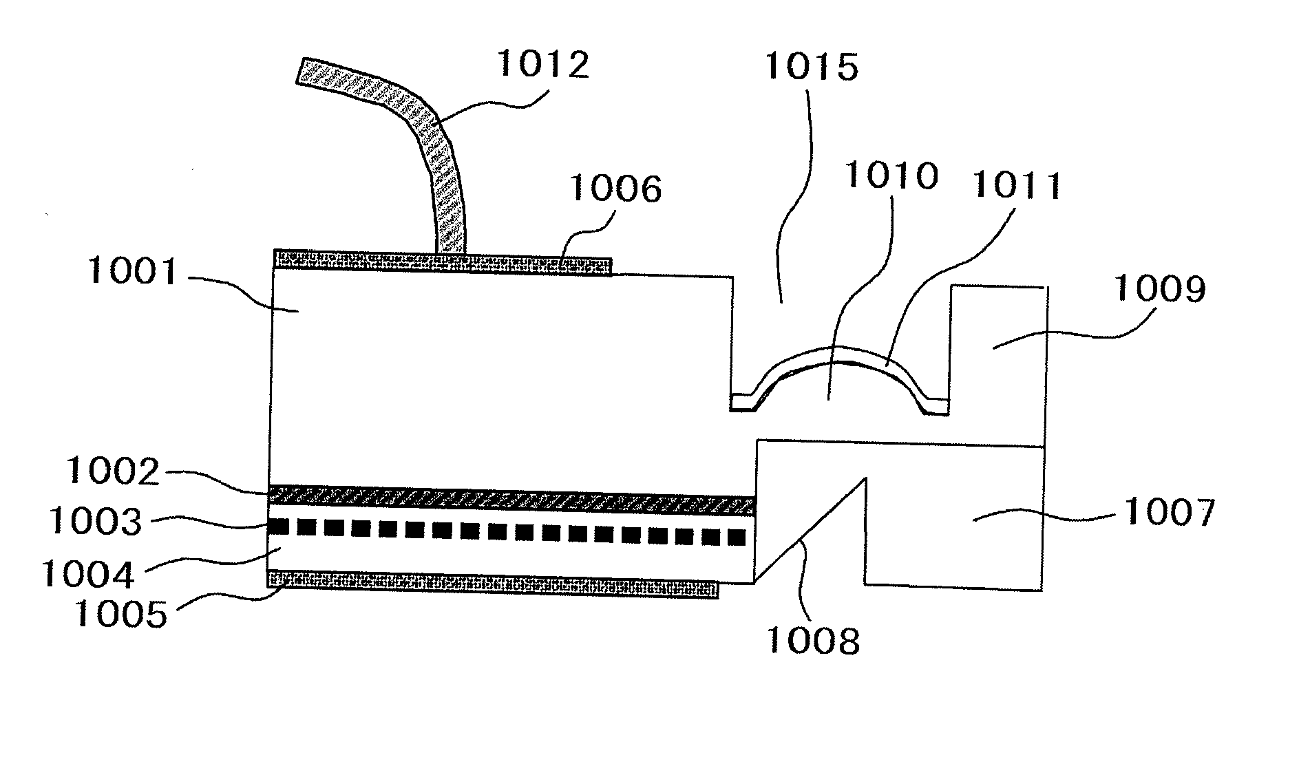
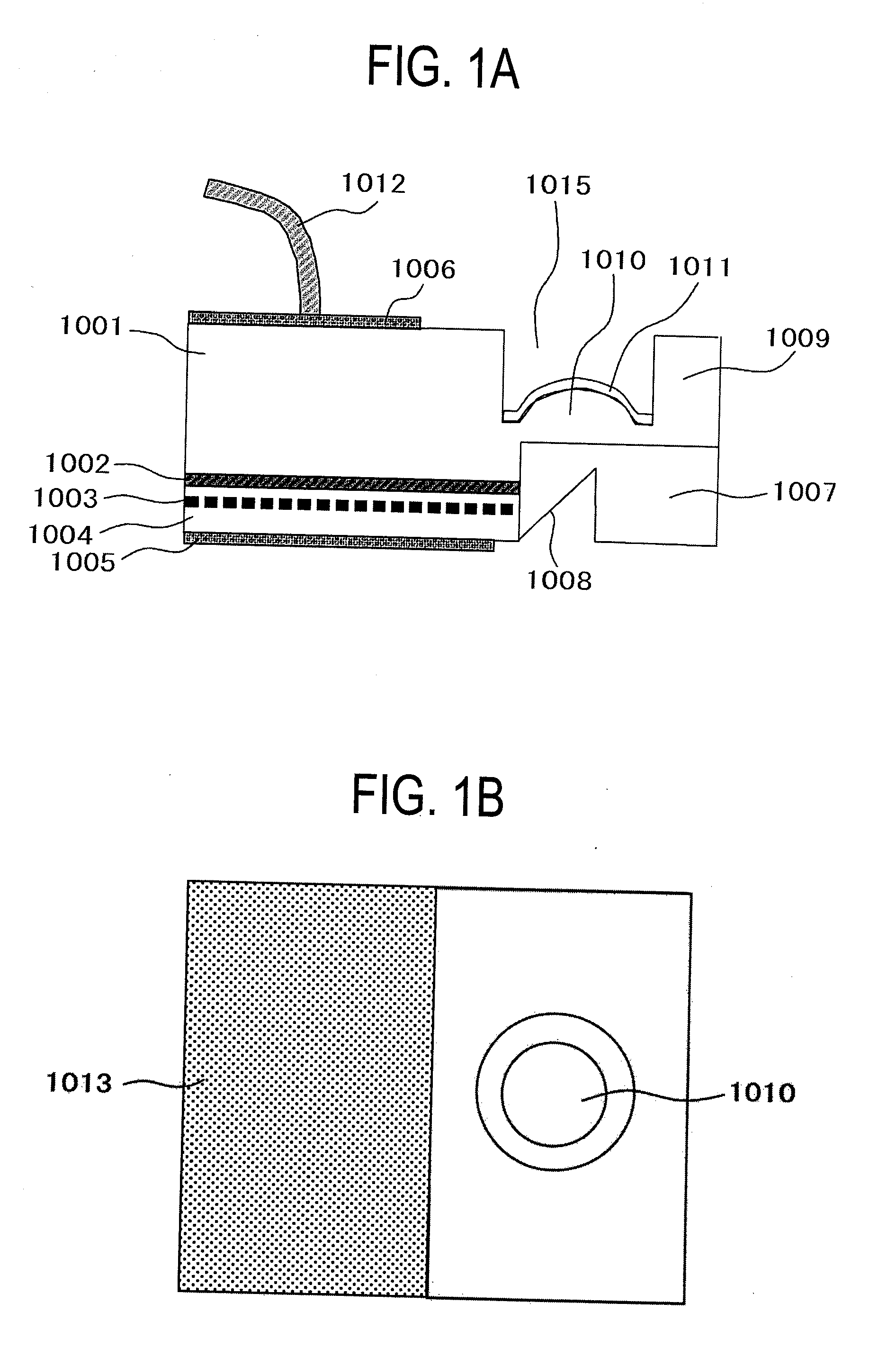
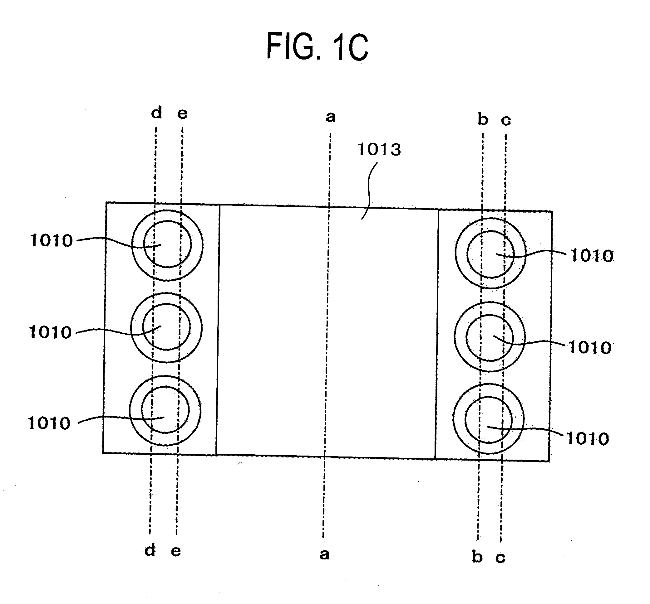
[0052]A structure of a horizontal cavity surface emitting laser according to a first embodiment will be explained using FIGS. 2A and 2B, FIGS. 3A through 3F, and FIG. 4. The present embodiment is an example in which the present invention is applied to a 250-μm horizontal cavity surface emitting laser in which a device width (lens interval) is the same value as the pitch of a commercialized ribbon fiber. FIG. 2A is a birds-eye view of the surface of a laser device, and FIG. 2B is a light emitting surface of the laser device. Incidentally, although a chip from which a single channel element is cut out is illustrated in FIGS. 2A and 2B, an array structure is also possible. In the horizontal cavity surface emitting laser according to the present embodiment, an active layer 2001, a p-type semiconductor layer 2002, and a p-type contact layer 2004 are successively stacked and grown over an n-type InP substrate 2000. Further, although not illustrated in the drawing, a diffraction grating la...

second embodiment

[0073]The present embodiment is an example applied to a 1.3 μm-band InGaAlAs quantum well type horizontal cavity surface emitting laser having an RWG-type flip-chip mounted structure with a device width of 250 μm. FIG. 5A is a birds-eye view showing the surface of a laser device, and FIG. 5B is a light emitting surface of the laser device. In the horizontal cavity vertically emitting laser according to the present embodiment, an n-type semiconductor layer 4001, an active layer 4002, a p-type semiconductor layer 4003, and a contact layer 4004 are successively stacked and grown over an Fe-doped semi-insulating semiconductor substrate 4000. Further, although not shown in the drawing, a diffraction grating layer is formed directly on the active layer 4002. n-doped InP is used for the n-type semiconductor layer 4001, p-doped InP is used for the p-type semiconductor layer 4003, and a strained quantum well structure of InGaAlAs or the like, for example is used for the active layer 4002. Ga...

third embodiment

[0074]The present embodiment is a configuration example where an array-type lens integration horizontal cavity vertically emitting laser fabricated by applying the present invention thereto is applied to a small module.

[0075]FIG. 6A is a sectional view taken along a device optical-axis direction, of a module, and FIG. 6B shows a top view of the module. In the module according to the present embodiment, a multilayer wiring ceramic substrate 6002 is mounted over a package substrate 6001 having a strip line by gold bumps 6009. Further, an integrated circuit 6003 for driving the laser, and a 4-channel lens integration type horizontal cavity vertically emitting laser array 6004 having a flip-chip mounted structure fabricated by applying the present invention thereto are mounted over the multilayer wiring ceramic substrate 6002 while being electrically connected to each other by gold bumps. Further, a fiber array connector 6005 to which a lens array 6006 is mounted, is mounted above the l...


PUM


Abstract

The horizontal cavity surface emitting laser includes a cavity structure portion including a stacked structure of a first conduction type clad layer, an active layer and a second conduction type clad layer stacked over a semiconductor substrate and causing light generated by the active layer to be reflected or resonated, an optical waveguide layer provided at part of the semiconductor substrate and guiding the light, a reflector provided in the optical waveguide layer, for reflecting the light and emitting the light from the back surface of the semiconductor substrate, and a condensing lens provided at the back surface thereof and focusing the reflected light. The back surface thereof has a groove provided with the condensing lens and a terrace-like portion disposed below the cavity structure portion and has a terrace shape with the cleavage direction along a longitudinal direction thereof provided along a cleavage direction of the semiconductor substrate.

Description

CLAIM OF PRIORITY[0001]The present application claims priority from Japanese patent application JP 2011-006630 filed on Jan. 17, 2011, the content of which is hereby incorporated by reference into this application.BACKGROUND OF THE INVENTION[0002]1. Field of the Invention[0003]The present invention relates to a semiconductor laser device used in optical communications, and relates to, for example, a horizontal cavity surface emitting laser and a manufacturing method thereof, and a photodiode.[0004]2. Description of the Related Arts[0005]With the development of information technologies, the transmission of data using optical fiber communications has been rapidly developed. An optical fiber communication technology has heretofore mainly been used in long-distance high-speed data transmission typified by a land trunk line or a submarine optical communication, an access communication network typified by FTTH (Fiber To The Home), and a metro network that connects trunk lines and an acces...

Claims


Application Information

Patent Timeline
Patent Type & Authority Applications(United States)
IPC IPC(8): H01S3/08H01L21/02G02B6/12H01S5/185
CPCG02B6/4214H01S5/0202H01S5/0207H01S5/0224H01S5/02284H01S5/42H01S5/12H01S5/18H01S5/2224H01S5/2226H01S5/0267H01L2224/16225H01L2924/15311H01S5/0234H01S5/02251H01S5/185
Inventor ADACHI, KOICHIROMATSUOKA, YASUNOBUSUGAWARA, TOSHIKISHINODA, KAZUNORITSUJI, SHINJI
Owner HITACHI LTD
Why Eureka
Try Eureka