Method for manufacturing a very-high-resolution screen using a nanowire-based emitting anisotropic conductive film

a technology of anisotropic conductive film and nanowire, which is applied in the direction of nanotechnology, electrical equipment, semiconductor devices, etc., to achieve the effect of large form factors

Active Publication Date: 2012-08-16
COMMISSARIAT A LENERGIE ATOMIQUE ET AUX ENERGIES ALTERNATIVES
View PDF2 Cites 45 Cited by
  • Summary
  • Abstract
  • Description
  • Claims
  • Application Information

AI Technical Summary

Problems solved by technology

A problem common to these two types of screen is the difficulty in combining high resolutions (many image points or pixels) with a small screen size (in order to reduce the cost).
In the case of LCD screens (in practice it is more precisely a matter of screens of the reflective LCOS (reflective “Liquid Crystal On Silicon” on integrated circuit) type or of the transmissive LCD on glass type (notably marketed by the Kopin company), one of the main problems for the small pixels is controlling the state of the liquid crystal between adjacent pixels.
In fact, the field lines created at the level of a pixel can affect the field lines of the adjacent pixels, generating interference at the level of these pixels.
A first problem arises regarding the deposit of the layers constituting the OLED diodes on the active matrix.
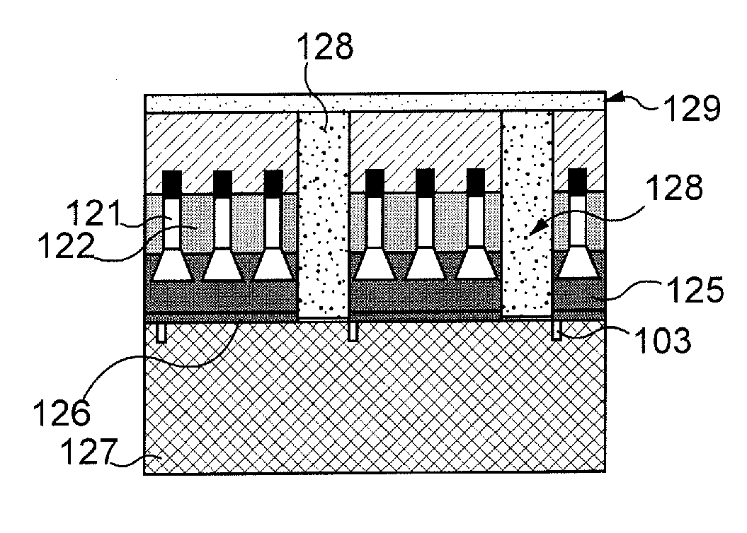
In fact, the pixel electrodes in practice constitute steps with respect to the surface of the active matrix; the fact that the emissive part is formed of layers causes these steps to remain in this emissive part; in particular the conductive layer forming the counter-electrode opposite the pixel electrodes (in practice it is a matter of the layer by which the emissive part terminates) thus comprises steps, which constitute risks of short-circuit (at the location of the level changes, the layers risk being interrupted and causing inadvertent contacts).
It is understood that this problem hampers the production of high-resolution (small pixel) OLED screens by causing the percentage of emissive surface to drop.
A second problem concerns with the use of colored filters.
In fact, whether these are deposited directly on the active matrix, or assembled with the active matrix, there is a loss of aperture related to the design rules in the first case, or related to the alignment precision in the second case.
This results in an additional limitation of the active surface aperture.
A third problem concerns the extreme fragility of the OLED layers, in particular with regard to impurities such as water for example.
Specific encapsulations are used but aging problems nevertheless persist with this type of screen.
In addition to the above mentioned difficulties is the problem that, whatever technique is used (LCD or OLED), the possible presence of particles at the interface between the active matrix and the emissive layers generates risks of horizontal short-circuit between adjacent pixels (which is a crippling risk which considerably hampers the reduction of inter-pixel pitches and therefore the resolution).
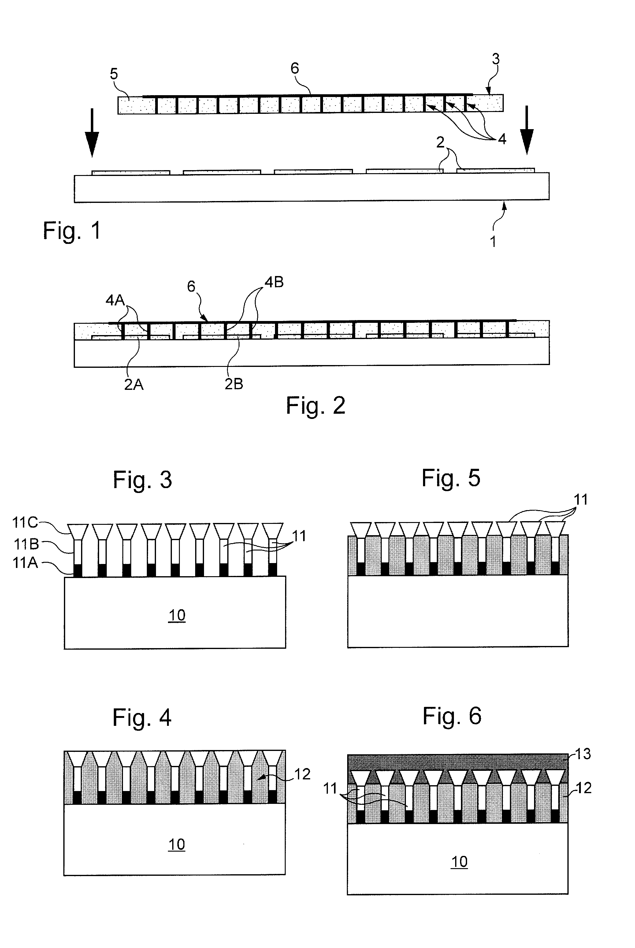
1. The first approach consists, starting from a solid substrate or from an epitaxial layer, in etching structures of nanowires, conventionally by means of a nano-lithographic and reactive plasma etching (ICP (Inductively Coupled Plasma), RIE (Reactive Ionic Etching), etc.) technique. This approach is notably described in the reference “InGaN-GaN Nanorod light Emitting Arrays Fabricated by Silica Nanomasks”; Min-Tann Hsieh and Al, IEEE journal of quantum electronics, Vol 44, pp 468-472, no. The etching approach therefore makes it possible to obtain wires of nanometric size with, however, certain limitations which depend on the nature of the material, the lithographic and etching methods, . . . , the advantage being that the orientation of the wires does not depend a priori on the crystalline orientation of the substrate.
2. The second approach consists in growing nanowires by chemical vapor deposition using a method of the VLS (Vapor Liquid Solidification) type which uses a generally metallic catalyst (gold for example). The nanowires often grow in epitaxial relationship with the substrate. Because of this, the vertical nanowires are obtained for a particular orientation of the substrate. The position and the diameter of the catalyst determine the position and the diameter of the nanowires, which can be less than 10 nm. This technique has certain advantages: very large form factors, control of dimensions of the nanowires, of the chemical composition and of the doping along the wires. There are also growth solutions without catalysts used for the generation of nanowires of GaN and ZnO or of heterostructures based on these materials by MOCVD (Metal Organic Chemical Vapor Deposition) and MBE (Molecular Beam Epitaxy) (see, in particular “High-Brightness Light Emitting Diodes Using Dislocation-Free Indium Gallium Nitride / Gallium Nitride Multiquantum-Well Nanorod Arrays”, Hwa-Mok et al, Nano Letters 2004, Vol 4, no.
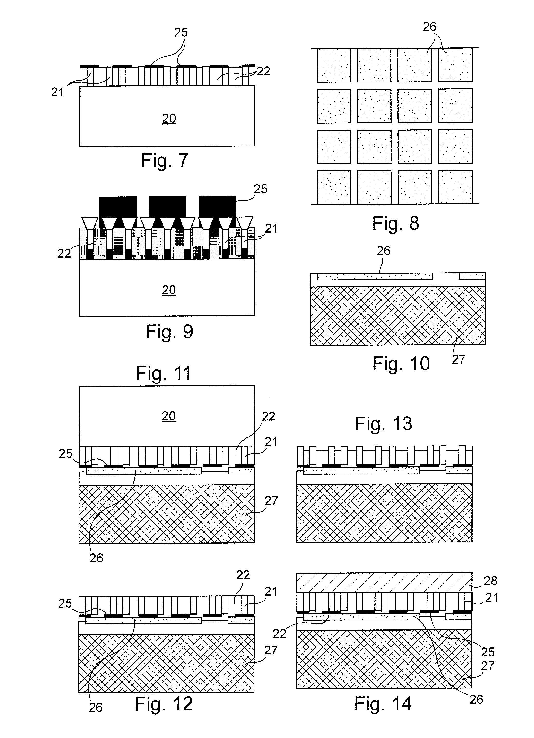
It should be noted that the arrangement of the second electrode beside the nanowires results from the difficulty there is in integrating a conductive or metal layer directly in the growth substrate of the wires (in fact it is not generally possible to implement a doping sufficient to allow the formation of such an electrode) without harming the epitaxial growth performance of nanowires and / or the overall performance of the final device.
It is clear that the presence of these lateral electrodes is an obstacle to the obtaining of high-resolution screens taking advantage of the virtual totality of their surface.
It is understood that the sets of nanowires are a source of fragility, both during their manufacture and within the assemblies in which they participate, since they are connected to each other only by the intermediary of the circuits to which they are fixed by their ends; moreover, their fixing to the second circuits requires accurate positioning of the latter with respect to the first circuits.
The proposals of this document therefore involve complex and costly procedures.

Method used


Image

  • Method for manufacturing a very-high-resolution screen using a nanowire-based emitting anisotropic conductive film
  • Method for manufacturing a very-high-resolution screen using a nanowire-based emitting anisotropic conductive film
  • Method for manufacturing a very-high-resolution screen using a nanowire-based emitting anisotropic conductive film

Examples


Embodiment Construction

[0056]Subjects, features and advantages of the invention will emerge from the following description, given as a non-limiting illustrative example with reference to the appended drawings in which:

[0057]FIG. 1 is a diagrammatic view of an emissive anisotropic substrate at the point of being assembled with an active pixel matrix,

[0058]FIG. 2 is a diagrammatic view of the assembly thus obtained,

[0059]FIG. 3 is a diagrammatic view of a first step of formation of the substrate shown in FIG. 1, implementing the formation of a homogeneous set of nanowires,

[0060]FIG. 4 is another diagrammatic view of it after encapsulation of the nanowires and planarization, typically by CMP, in order to make flush the edges of the wires,

[0061]FIG. 5 is another diagrammatic view of it after baring the ends of the nanowires,

[0062]FIG. 6 is another diagrammatic view of it after deposition of a conductive layer connected to said ends,

[0063]FIG. 7 is a diagram of an emissive anisotropic substrate based on nanowi...


PUM


Abstract

A method for producing an emissive pixel screen includes forming an active pixel matrix along which an electrode forming layer runs and having pixels arranged according to a distribution, forming an anisotropic substrate that includes a set of light emitting diodes constituted by parallel nanowires and arranged in an insulating matrix transversely with respect to a substrate thickness and having a density higher than a density of the pixels irrespective of the pixel distribution, connecting the substrate to the active pixel matrix by connecting only sub-groups of the parallel nanowires by a first end to separate pixel electrodes defined in the electrode forming layer according to the distribution of the pixels in the matrix, and connecting the sub-groups, by another end, to a common electrode, and delimiting the sub-groups by rendering the nanowires of the substrate that are arranged between the sub-groups emissively inactive.

Description

FIELD OF THE INVENTION[0001]The invention relates to the production of very-high-resolution emissive screens (with fixed pixels), whose pixel size is preferably at most equal to one micron; it can be a matter of small-sized screens (the term “micro-screens” is sometimes used) and / or of flexible screens. These screens, which can be flat (even if they have a certain curvature), are produced on integrated circuit active matrices, in practice made of silicon.PRIOR ART AND DISADVANTAGES[0002]At present there are two types of high-resolution electro-optical screens: LCD (Liquid Crystal Display) screens—see in particular the document U.S. Pat. No. 6,052,162—and OLED (Organic Light Emissive Diodes) screens—see in particular the document WO-2007 / 085554. It can be noted that, unlike OLED screens, LCD screens are not emissive screens.[0003]A problem common to these two types of screen is the difficulty in combining high resolutions (many image points or pixels) with a small screen size (in ord...

Claims


Application Information

Patent Timeline
Patent Type & Authority Applications(United States)
IPC IPC(8): H01L33/04B82Y40/00B82Y99/00
CPCB82Y20/00H01L27/156H01L33/18H01L33/0079H01L2924/0002H01L33/08H01L2924/00H01L33/0093
Inventor TEMPLIER, FRANCOISCLAVELIER, LAURENTRABAROT, MARC
Owner COMMISSARIAT A LENERGIE ATOMIQUE ET AUX ENERGIES ALTERNATIVES
Why Eureka
Try Eureka