Method of treating an oxidized layer of metal nitride
- Summary
- Abstract
- Description
- Claims
- Application Information
AI Technical Summary
Benefits of technology
Problems solved by technology
Method used
Image
Examples
Embodiment Construction
[0050]For clarity, the same elements have been given identical reference numerals. Further, only those elements that are essential to understanding the invention are shown, and they are shown in diagrammatic manner and not to scale.
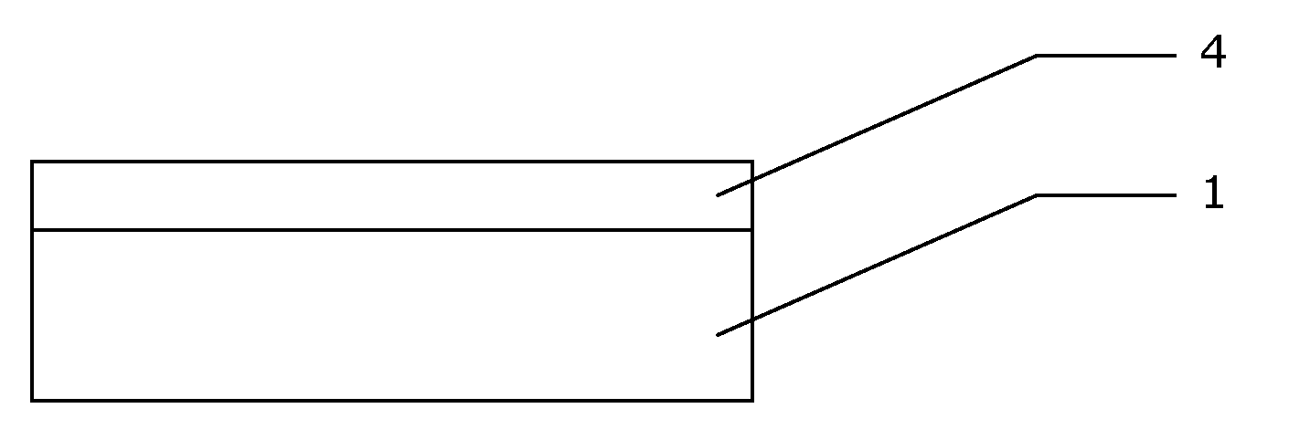
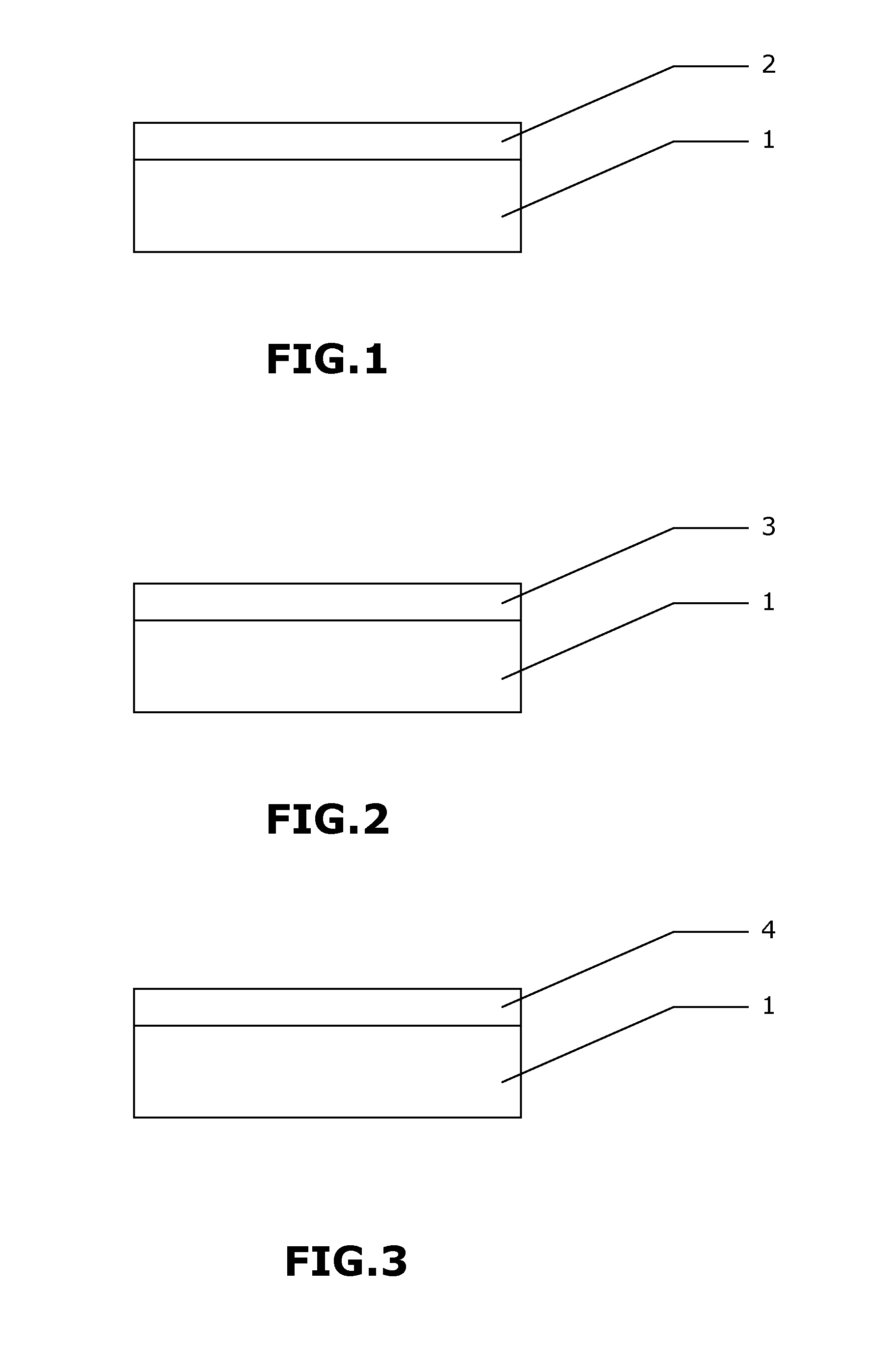
[0051]FIG. 1 shows a stack of at least two layers having a circular cross-section with a diameter of 200 mm [millimeter] before applying the treatment method of the present invention. These two layers were a first layer of titanium nitride (1) with a thickness of 80 Å, the upper portion of which was covered with a layer of titanium oxide (2) with a thickness of approximately 40 Å. The total thickness of these two layers was thus 120 Å.
[0052]Said stack was deposited on the chuck of a plasma reactor supplied by Tokyo Electron Limited, with the reference 85 SCCM. Clearly, the first layer of nitride was not in direct physical contact with the chuck. Said stack was originally deposited on a wafer of a substrate of semiconductor material (not shown in FIGS. 1 t...
PUM
| Property | Measurement | Unit |
|---|---|---|
| Temperature | aaaaa | aaaaa |
| Temperature | aaaaa | aaaaa |
| Temperature | aaaaa | aaaaa |
Abstract
Description
Claims
Application Information

