Ir emitter and ndir sensor

Active Publication Date: 2012-10-25
SCIOSENSE BV
View PDF7 Cites 71 Cited by
  • Summary
  • Abstract
  • Description
  • Claims
  • Application Information

AI Technical Summary

Benefits of technology

[0035]In another embodiment of the invention, an IR detector is integrated on the same chip as the IR source. The IR detector consists of either a thermopile or an array of thermodiodes or thermotransistors on a membrane. If the detector is a thermopile it can consist of one or more thermocouples connected in series with one junction inside the membrane and one outside. The two thermocouple materials may consist of p or n doped single crystal silicon, n or p doped polysilicon or a metal (such as tungsten). If thermodiodes are used they may consist of a P+/N+ junction, or may have a p or n type well or drift region between. The diodes can be connected as an array to improve the sensitivity. Thermodiodes in particular have the advantage that their temperature coefficient is constant for high temperatures up to 500° C. Circuitry can be integrated on-chip to process the detector signal. Similarly thermotransistors are made in CMOS technology using bipolar npn or pnp structures with at least one junction shorted. The thermodiode or thermotransistors or circuits b

Problems solved by technology

Moreover, wafer bonding is used to encapsulate the heater in vacuum (which adds extra fabrication steps and increases the manufacturing cost).
The use of polysilicon in all these designs reduces the stability of the device as polysilicon resistance drifts in time at high temperatures above 400° C.
This device is not envisaged to be fabricated in a CMOS process, and the construction of the device also does not lend itself to be fabricated in a CMOS process.
These extra processing steps add to the fabrication cost of the device.
Platinum is however not CMOS compatible and its use in CMOS foundries is prohibited, as it acts as a deep dopant and can contamina

Method used


Image

  • Ir emitter and ndir sensor
  • Ir emitter and ndir sensor
  • Ir emitter and ndir sensor

Examples


Example

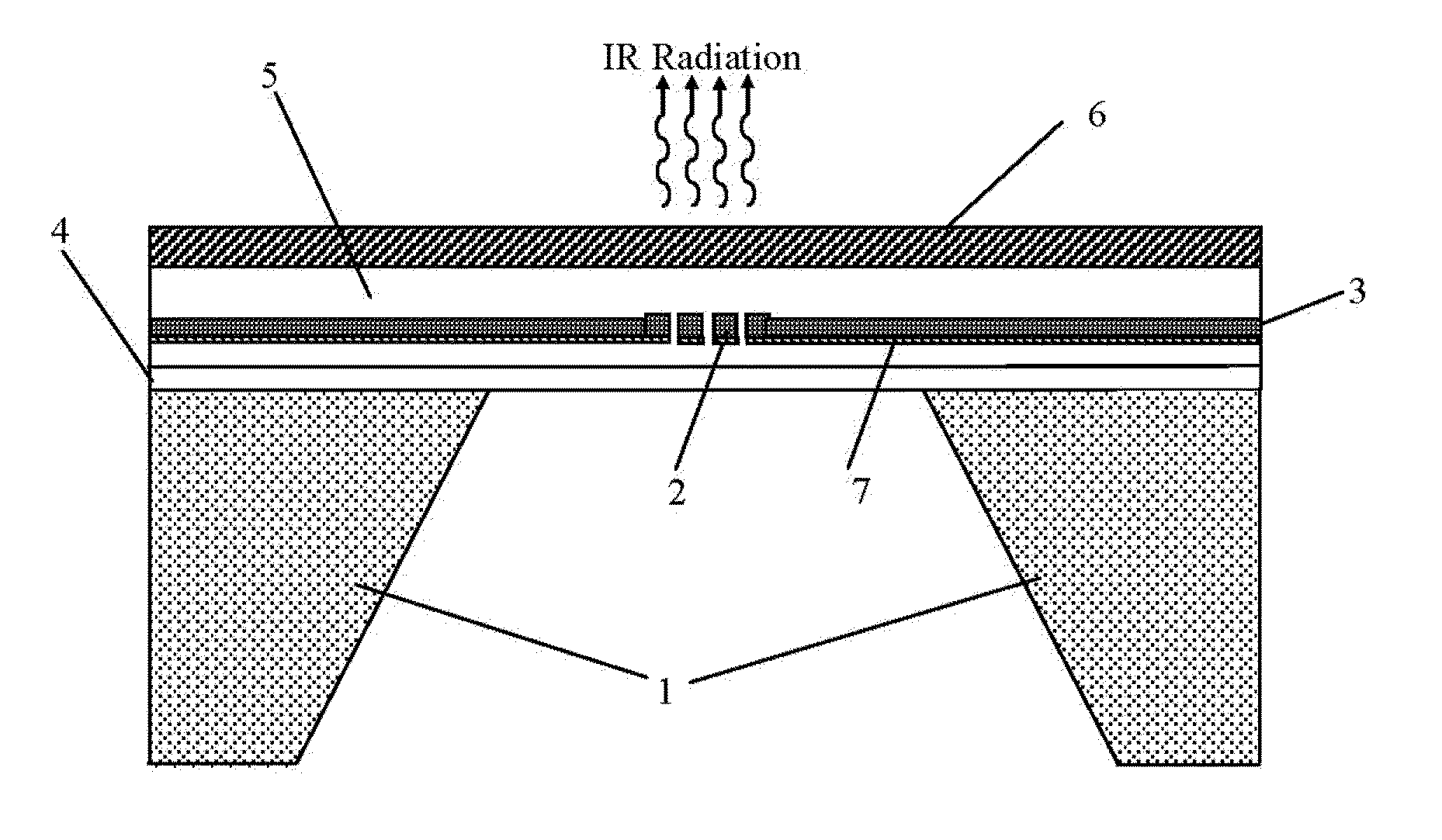
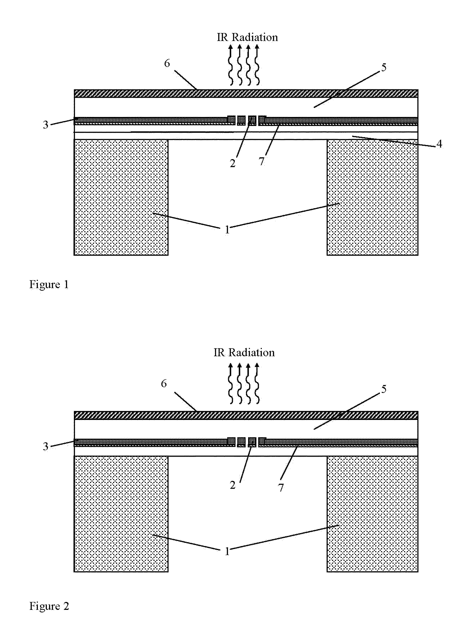
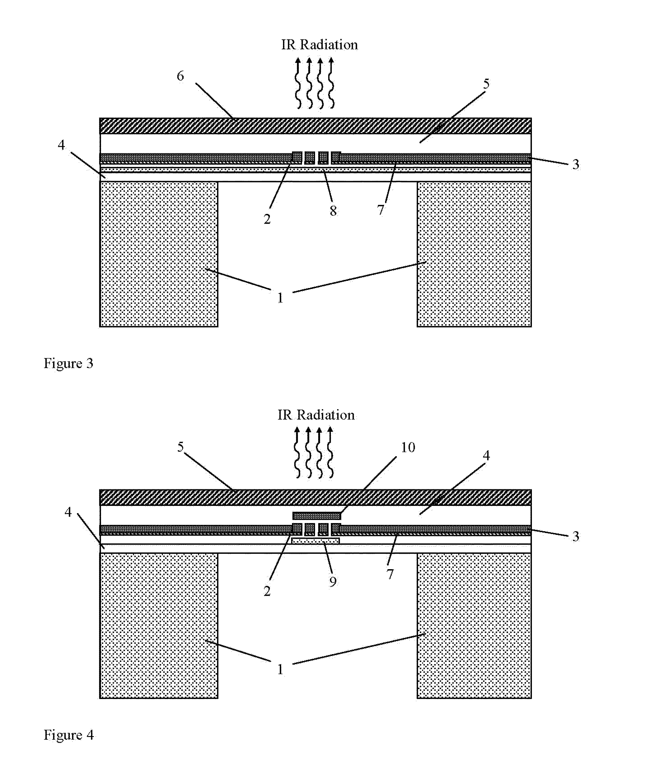
[0057]Embodiments of the present invention seek to improve on the state of the art devices by using a CMOS layer of tungsten both as part of a heater which emits infrared radiation and an interconnect metal for electronic devices. The IR emitter is embedded into a dielectric membrane defined by etching the silicon substrate. The etching may be done by a Deep Reactive Ion (DRIE) technique. Such a device can operate reliably at high temperatures (well above 600° C.) due to the use of the tungsten heater. Moreover the use of the tungsten layer within a CMOS process ensures very high stability, long term reliability and high reproducibility. This is in contrast to heaters fabricated by other techniques than CMOS such as screen printing. To further improve the reliability, the tungsten heater may have a titanium / titanium nitride liner. Furthermore, the use of the CMOS technology to fabricate the device results in lower fabrication costs and allows circuitry to be integrated on the same c...


PUM


Abstract

An IR source in the form of a micro-hotplate device including a CMOS metal layer made of at least one layer of embedded on a dielectric membrane supported by a silicon substrate. The device is formed in a CMOS process followed by a back etching step. The IR source also can be in the form of an array of small membranes—closely packed as a result of the use of the deep reactive ion etching technique and having better mechanical stability due to the small size of each membrane while maintaining the same total IR emission level. SOI technology can be used to allow high ambient temperature and allow the integration of a temperature sensor, preferably in the form of a diode or a bipolar transistor right below the IR source.

Description

RELATIONSHIP TO EARLIER APPLICATIONS[0001]This application is a continuation-in-part of U.S. application Ser. No. 12 / 691,104 filed on Jan. 21, 2010, which is hereby incorporated by reference in its entirety.FIELD OF THE INVENTION[0002]This invention relates to a thermal Infra-Red (IR) source using a micro-hotplate fabricated on a microchip. The invention also relates to integrating the IR source with an IR detector to make an NDIR sensor.BACKGROUND TO THE INVENTION[0003]It is known to fabricate a thermal IR source on a silicon substrate consisting of a micro-heater formed within a thin membrane layer (made of electrically insulating layers) that is formed by etching part of the substrate. Such devices can be used to provide heat (e.g. 600° C.) with low power consumption (typically from a few mW to hundreds of mW) for use as infra-red sources / emitters.[0004]For Example, Parameswaran et. al. “Micro-machined thermal emitter from a commercial CMOS process,” IEEE EDL 1991 reports a polys...

Claims


Application Information

Patent Timeline
IPC IPC(8): G01N21/61G21K5/02H01L21/02B82Y15/00
CPCH05B2203/032H05B3/267G01J3/108
Inventor UDREA, FLORINGARDNER, JULIANALI, SYED ZEESHANCHOWDHURY, MOHAMED FOYSOLPOENARU, ILIE
Owner SCIOSENSE BV
Why Eureka
Try Eureka