Electroplating apparatus and method

a technology of electroplating apparatus and substrate, which is applied in the direction of electrolysis process, electrical apparatus, electrolysis components, etc., can solve the problems of insufficient development of appropriate etching solution for etching copper film in order to form the gate electrode and the gate line, delay and distortion of the gate signal and data signal, etc., to minimize the processing time and minimize the alignment error

Inactive Publication Date: 2012-11-29
JOO SEUNG KI
View PDF10 Cites 9 Cited by
  • Summary
  • Abstract
  • Description
  • Claims
  • Application Information

AI Technical Summary

Benefits of technology

[0066]As described above, an electroplating apparatus and method according to the present invention can form a metal thin film uniformly on a large substrate.
[0067]In addition, when a bottom gate is formed of copper with a low resistance value that is appropriate for a large display by an electroplating method, an electrolyte is coated on seed layers formed on a substrate so as to be supported by surface tension and a copper plate that is an anode is made to move along the seed layers, to thus electrodeposite copper wires thereon.
[0068]In addition, the electroplating apparatus and method according to the present invention does not require for a large device that contains an electrolyte and enables copper to be electrodeposited uniformly.
[0069]Therefore, in the case of an electroplating apparatus and method according to the present invention, copper with a low resistance value that is suitable for a large display is selectively formed quickly into a thickness usable for a bottom gate according to an electroplating method, to thereby minimize a processing time and simultaneously omit a copper etching process.
[0070]In addition, the present invention can solve a step coverage problem without passing through a planarization process by selectively forming a trench type copper bottom gate structure using copper that is used as a gate electrode.
[0071]Furthermore, since the present invention uses copper for a gate electrode, a source region and a drain region can be automatically aligned with respect to a gate by back exposure without using a separate mask, to thereby minimize an alignment error.

Problems solved by technology

As a result, a gate signal and a data signal have been delayed and distorted.
Since it is difficult to lower resistance of a gate wire of a thin film transistor (TFT) in comparison with that of a data wire, among the gate and data wires, it is required to use copper as the gate wire.
However, an appropriate etching solution that is used for etching a copper film in order to form the gate electrode and gate line has not been developed.
Further, there is a problem that an etching process for etching the copper film produces heavy metals causing an environmental pollution.
Unlike the above-described metal and metal alloys, copper does not constitutes fluoride or chloride, there is a problem that copper is not well etched.
In addition, in the case that copper is piled up with a thick thickness in order to reduce resistance, there is a problem that it takes 3-4 hours or longer as a processing time.
However, it takes long time to form a copper thick film of such a thickness.
Further, in the case that a gate electrode structure of a thick film is employed, a gate insulation film that is directly formed on the upper portion of a gate electrode by a well-known process may cause a step coverage problem.
According to the conventional electrodeposition technology, it is not possible to form a uniform copper film on the entire surface of the substrate because of high resistance in the case of a large area display.
As a result, the Korean Patent Laid-open Publication No. 10-2006-115522 has the same problem as that of the conventional art at the time of etching the copper metal layer.
In addition, the technology disclosed in the Korean Patent Laid-open Publication No. 10-2006-115522 may cause a step coverage problem in a subsequent process of forming the gate electrode as a thick film of one micrometer or more thick, and does not present any related solutions.
Accordingly, an alignment error of 2 to 4 micrometers may be caused.
Further, such an alignment error cannot be equally distributed to both ends of a channel region and leans toward one end of the channel region, to thereby become a factor of aggravating an electrical performance of the thin film transistor (TFT).
However, in the case of a large substrate whose one side is two or more meters long, a problem such as a voltage drop may be caused.
Accordingly, it is difficult to electroplate a metal film of uniform thickness on the large substrate.
In addition, the copper electroplating process requires that a container containing an electrolyte should be large in itself, and a huge amount of the electrolyte should be needed, to accordingly cause many industrial problems.
Moreover, when the electroplating is utilized in a semiconductor manufacturing process, a problem bigger than that of maintaining uniformity in thickness of an electrodeposited metal film is regulation of grain size.
Thus, since surface roughness of a few micrometers may also cause a big problem in the semiconductor manufacturing process, grain size should become a micrometer level or less unlike typical applicable cases.
Meanwhile, in the case of using the conventional typical wet copper plating system that dips a large-area substrate whose electrodeposition area is wide like a large display substrate whose one side is two meters or more long, in order to perform a copper plating process, the metal electrode 150 that is used as the cathode may cause a big difference in electric current densities between a portion “a” close to a power supply and a portion “b” far from the power supply, due to a voltage drop across resistance values of the portions “a” and “b.”
However, since nucleation does not occur well at a portion of a low current density, a phenomenon that grain size becomes large occurs as the portion “b” of FIG. 2.
Thus, in the case of using a large tub that can contain a large display substrate, it is extremely difficult to control such many variables.
As a result, in the case that copper plating is performed on a large-area substrate by using the conventional wet plating method employing the conventional dipping process, grain of a plated copper film is not formed into a uniform size.

Method used


Image

  • Electroplating apparatus and method
  • Electroplating apparatus and method
  • Electroplating apparatus and method

Examples


first embodiment

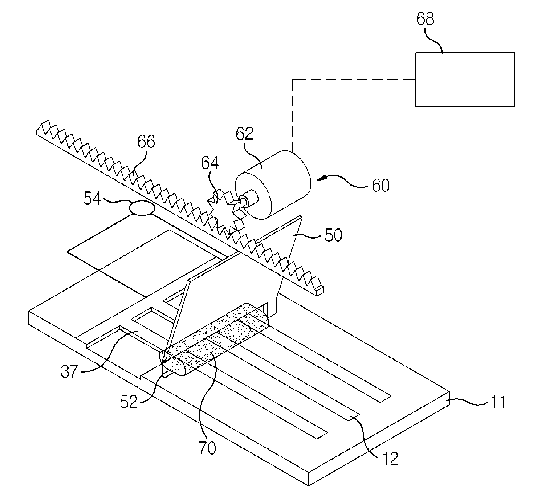
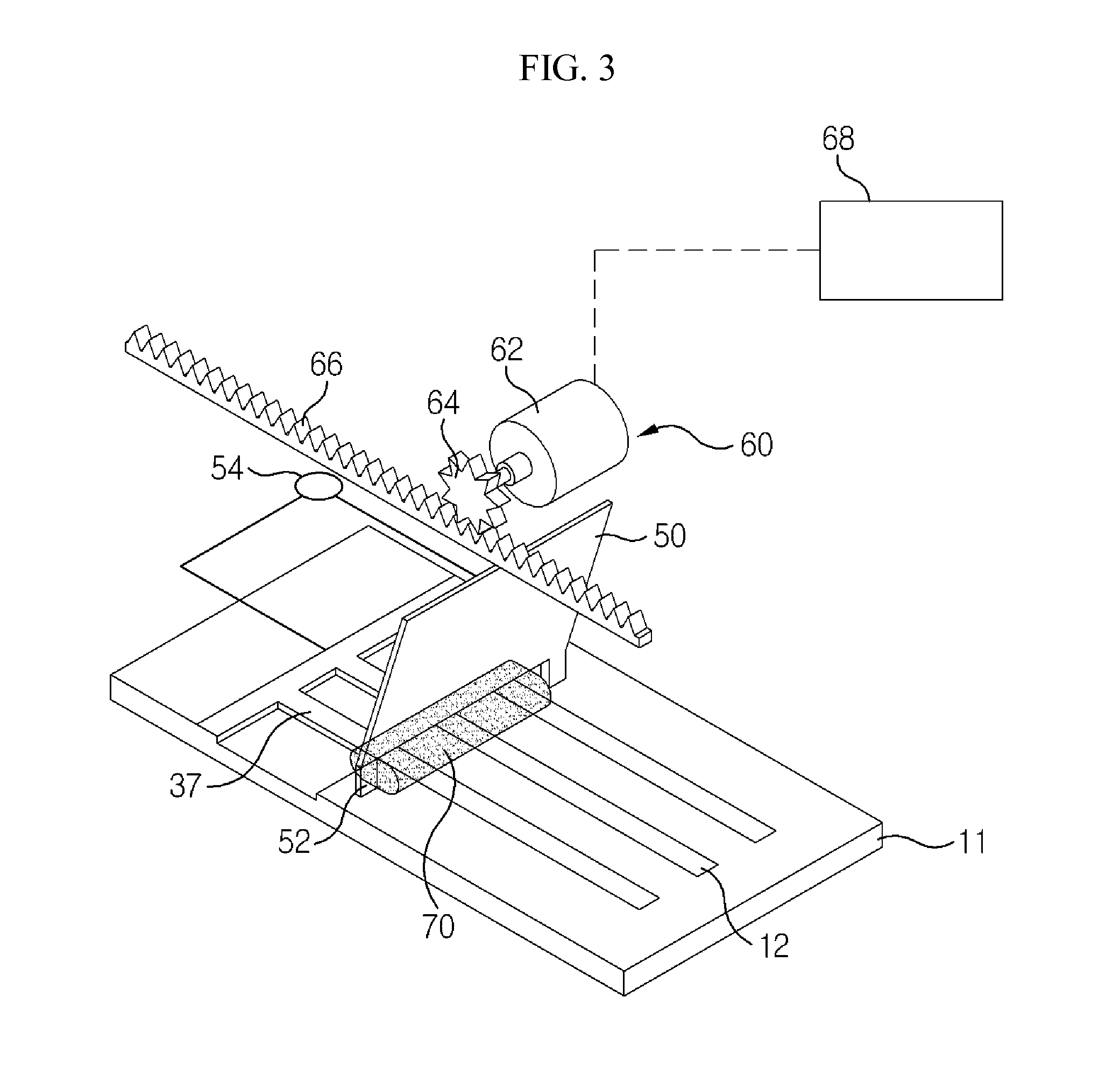
[0081]FIG. 3 is a perspective view showing an electroplating apparatus according to the present invention.

[0082]Referring to FIG. 3, the electroplating apparatus according to the first embodiment according to the present invention includes: a copper electrode plate 50 that is disposed so as to move along a rectilinear line on an upper surface of an insulating substrate 11 on which seed electrodes 12 are formed; a driving unit 60 that makes the copper electrode plate 50 move reciprocally along a rectilinear line; and a power supply 54 that applies electric current between the copper electrode plate 50 and each of the seed electrodes 12.

[0083]A method of forming the seed electrodes 12 on the insulating substrate 11 will follow in detail.

[0084]In the case that the insulating substrate 11 is formed of a hydrophobic material, an electrolyte 70 does not spread but forms on the surface of the insulating substrate 11. As a result, the electrolyte 70 stay between the copper electrode plate 5...

second embodiment

[0102]FIG. 4 is a perspective view showing an electroplating apparatus according to the present invention.

[0103]Referring to FIG. 4, the electroplating apparatus according to the second embodiment of the present invention includes: a copper electrode plate 50 that is disposed so as to move along a rectilinear line on an upper surface of an insulating substrate 11 on which seed electrodes 12 are formed; a pushing plate 56 that is disposed at the rear side of the copper electrode plate 50 to thus push an electrolyte 70 that is placed at the rear side of the copper electrode plate 50 toward the copper electrode plate 50; a driving unit 60 that makes the copper electrode plate 50 and the pushing plate 56 move along a rectilinear line; and a power supply 54 that is connected between the copper electrode plate 50 and each of the seed electrodes 12 and thus applies electric current between the copper electrode plate 50 and each of the seed electrodes 12.

[0104]If the insulating substrate 11...

third embodiment

[0111]FIG. 5 is a perspective view showing an electroplating apparatus according to the present invention.

[0112]Referring to FIG. 5, the electroplating apparatus according to the third embodiment of the present invention includes: a copper electrode plate 50 that is disposed so as to move along a rectilinear line on an upper surface of an insulating substrate 11 on which seed electrodes 12 are formed; an electrolyte supplier 80 that is disposed at the front side of the copper electrode plate 50 to thus supply an electrolyte 70 on the surface of the insulating substrate 11; an electrolyte remover 90 that is disposed at the rear side of the copper electrode plate 50 to thus remove the electrolyte from the copper electrode plate 50; a driving unit 60 that makes the copper electrode plate 50, the electrolyte supplier 80 and the electrolyte remover 90 move along a rectilinear line; and a power supply that is connected between the copper electrode plate 50 and each of the seed electrodes ...


PUM

PropertyMeasurementUnit
total lengthaaaaaaaaaa
thickaaaaaaaaaa
thickaaaaaaaaaa

Abstract

Provided is an electroplating apparatus including: a copper electrode plate that is disposed with a gap from an upper surface of an insulating substrate on which seed electrodes are formed; a driving unit that makes the copper electrode plate move along a rectilinear line; a power supply that applies electric current between the copper electrode plate and each of the seed electrodes; and spacers that are provided on the lower surface of the copper electrode plate to thereby make an electrolyte stay by surface tension between the copper electrode plate and the insulating substrate, and that maintains the gap between the copper electrode plate and the insulating substrate so that the electrolyte may move together with the copper electrode plate. Accordingly, a uniform copper film can be formed on the surface of a large substrate.

Description

CROSS-REFERENCE TO RELATED APPLICATION[0001]This application claims the benefit of Korean Patent Application No. 10-2011-0050343, filed on May 26, 2011; and Korean Patent Application No. 10-2011-0065375, filed on Jul. 1, 2011, in the Korean Intellectual Property Office, the disclosure of which is incorporated herein by reference.BACKGROUND OF THE INVENTION[0002]1. Field of the Invention[0003]The present invention relates to an apparatus for forming a metal thin film on a substrate, and more particularly, to an electroplating apparatus and method that can uniformly form a metal thin film on a large substrate.[0004]2. Description of the Related Art[0005]In general, various kinds of metal and metal alloys such as aluminum (Al), molybdenum (Mo), and molybdenum-tungsten (MoW) are used as a gate electrode constituting a bottom gate of a thin film transistor (hereinafter referred to TFT). The reason why the aluminum (Al), molybdenum (Mo), molybdenum-tungsten (MoW), etc., are used as a mate...

Claims


Application Information

Patent Timeline
Patent Type & Authority Applications(United States)
IPC IPC(8): C25D5/04C25D5/00
CPCC25D5/04C25D5/02C25D17/12C25D5/22C25D17/10C25D5/10C25D5/617H01L21/288H01L21/28
Inventor JOO, SEUNG KI
Owner JOO SEUNG KI
Why Eureka
Try Eureka