
Al alloy film for use in display device

Inactive Publication Date: 2012-11-29
KOBE STEEL LTD
View PDF8 Cites 10 Cited by
  • Summary
  • Abstract
  • Description
  • Claims
  • Application Information

AI Technical Summary

Benefits of technology

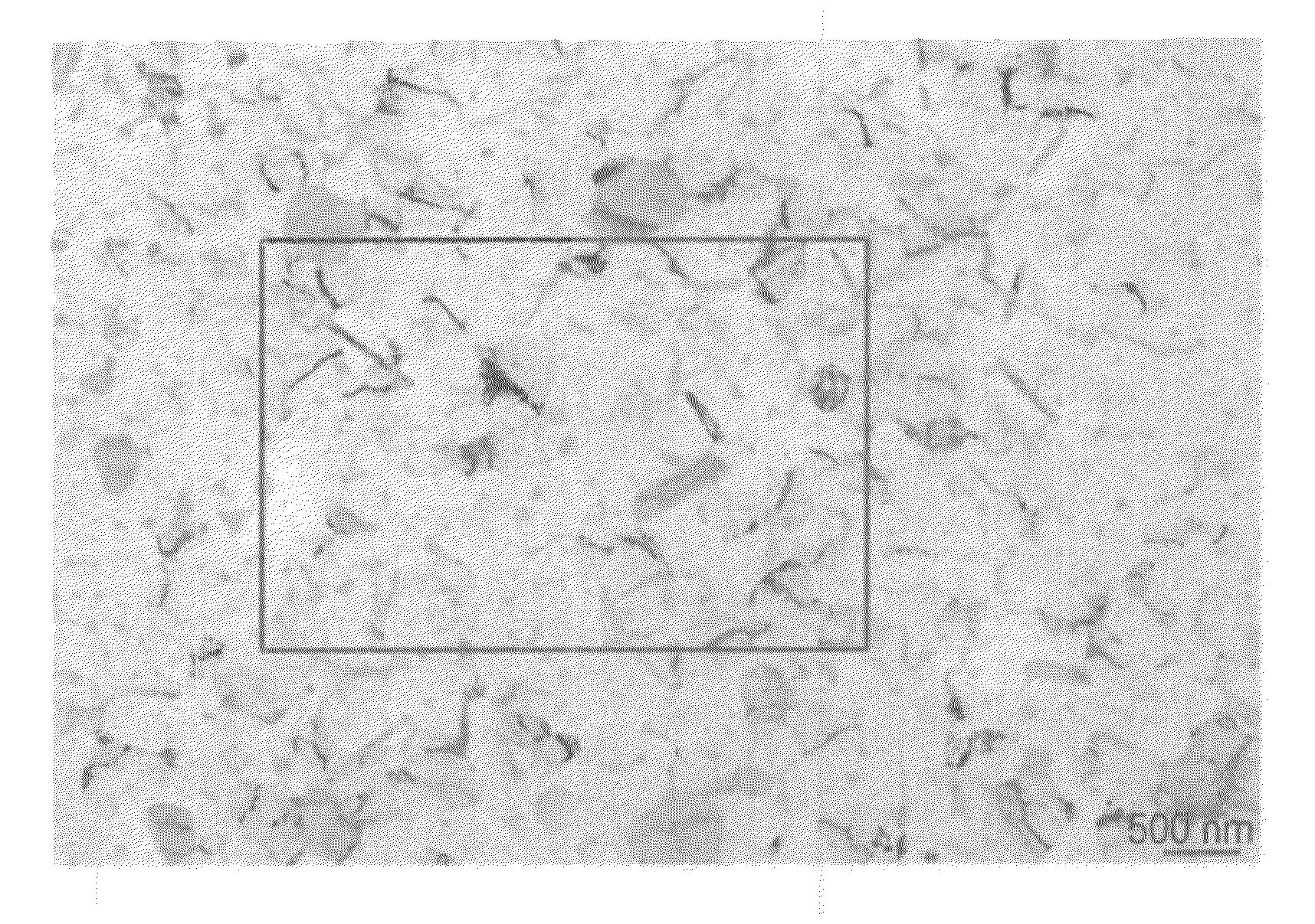
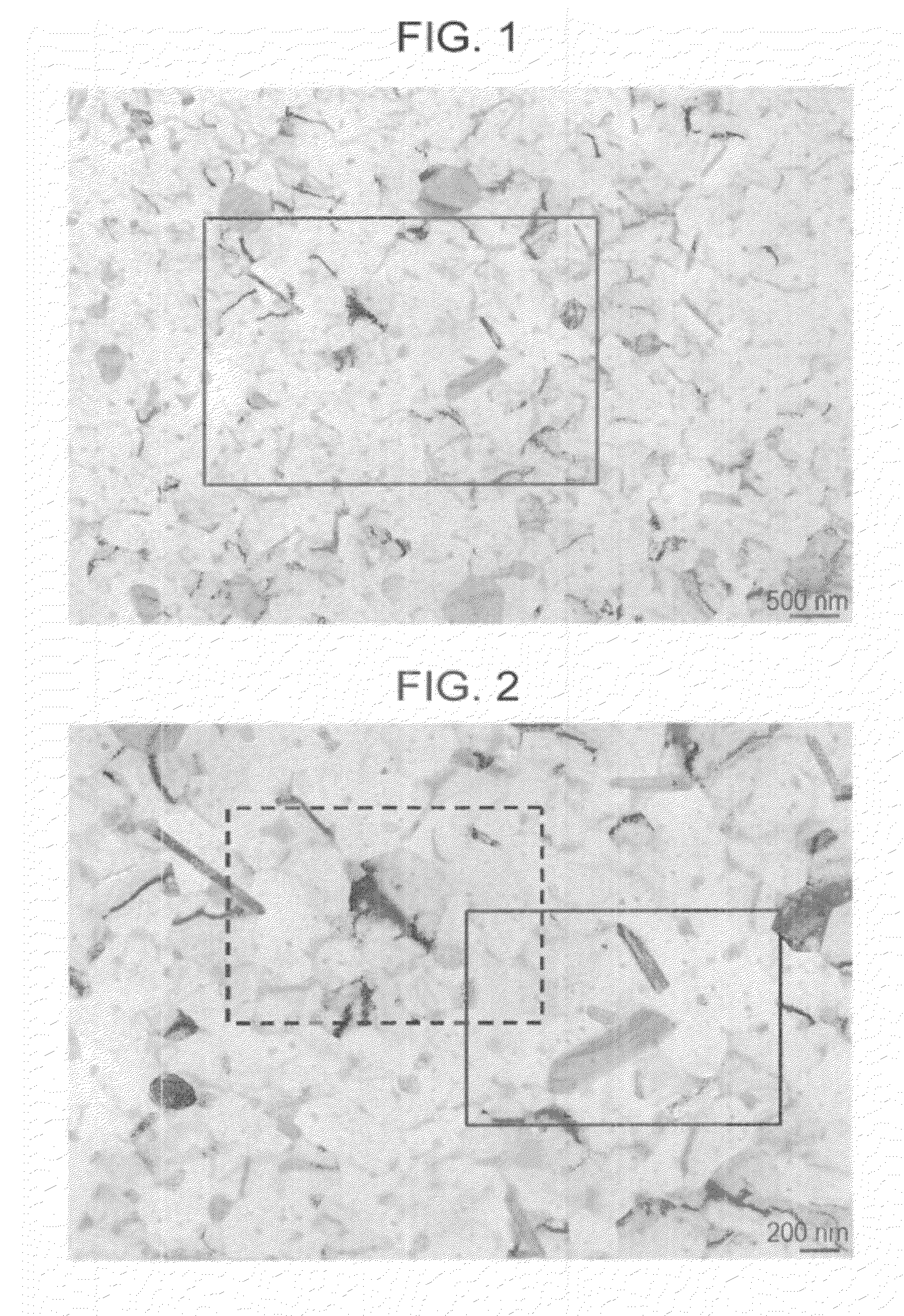
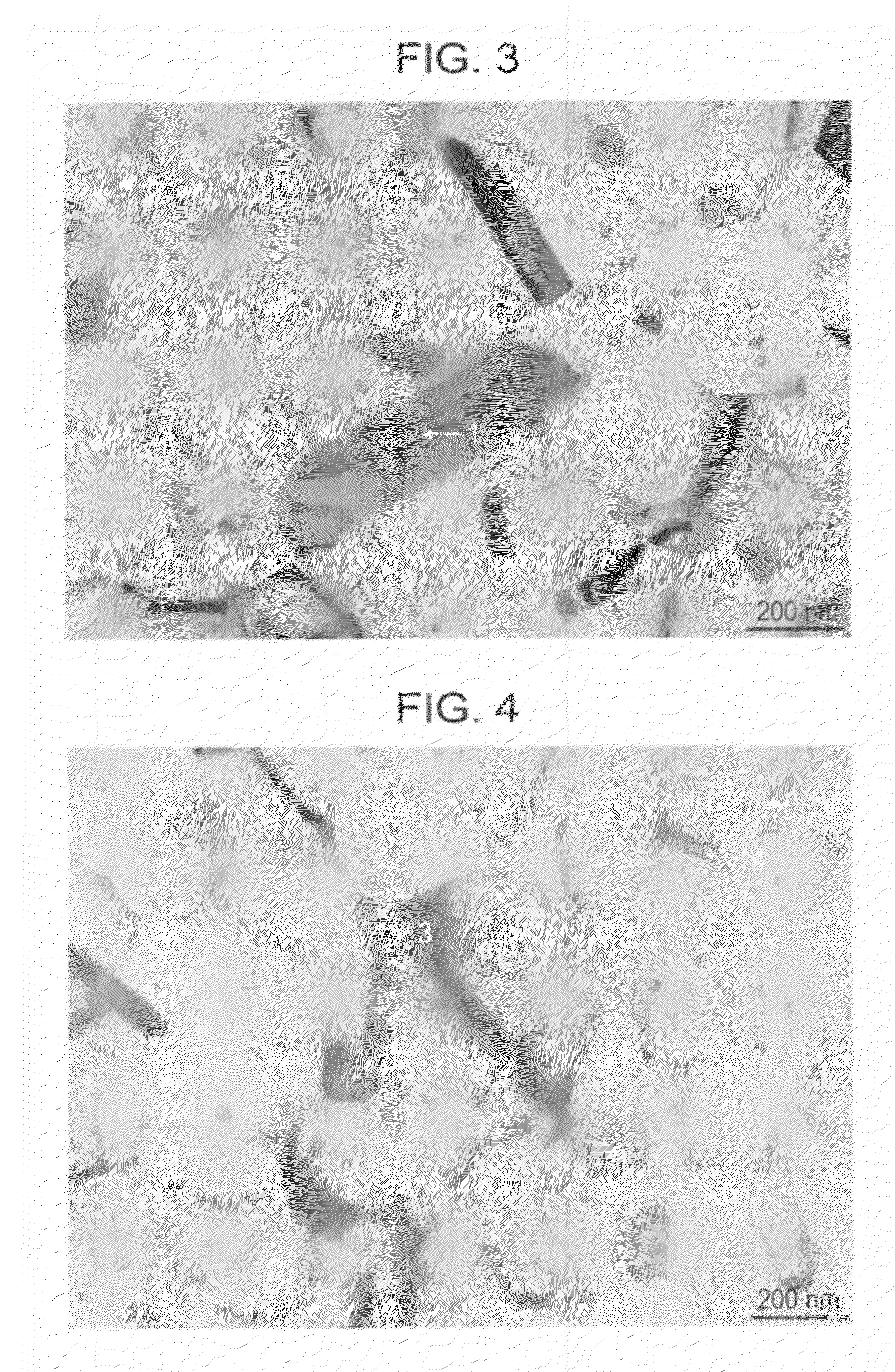
[0029]A first Al alloy film (Al-group X element-rare-earth element alloy) according to the present invention is composed of predetermined alloy elements and a first precipitate. Thus, the first Al alloy film has excellent heat resistance when exposed to a high temperature of about 450° C. to about 600° C., and has satisfactory resistance to alkaline corrosion and low electrical resistance (wiring resistance) after high-temperature treatment. Preferably, a second Al alloy film (Al-group X element-rare-earth element-Cu / Ge alloy) according to the present invention is composed of predetermined alloy elements, the first precipitate, and a second precipitate. Thus, the second Al alloy film has higher heat resistance. More preferably, a third Al alloy film (Al-group X element-rare-earth element-Ni / Co—Cu / Ge alloy) according to the present invention is composed of predetermined alloy elements, the first precipitate, the second precipitate, and a third precipitate. Thus, high stripping solution resistance under the high temperature described above and low contact resistance with a transparent conductive film can be provided in addition to the foregoing properties. It is therefore possible to directly connect the Al alloy film to the transparent conductive film.
[0030]According to the present invention, in particular, in a process for producing a thin-film transistor substrate including semiconductor layers composed of polycrystalline silicon and continuous grain silicon, when the substrate is exposed to a harsh high-temperature environment in which high-temperature heat treatment at about 450° C. to about 600° C. is performed and even when the high-temperature heat treatment is performed at least twice, carrier mobilities in the semiconductor silicon layers are increased, thereby improving the response speed of a TFT. It is thus possible to provide a high-performance display device that can achieve power savings and support high-speed moving images.

Problems solved by technology

Similarly, PTL 3 describes evaluation results of heat resistance at 230° C. and 300° C. However, heat resistance when heat treatment is performed at a higher temperature is not evaluated at all.

Method used


Image

  • Al alloy film for use in display device
  • Al alloy film for use in display device
  • Al alloy film for use in display device

Examples


example 1

[0099]Al alloy films (thickness: 300 nm) having various alloy compositions described in Tables 1 to 7 were formed by a DC magnetron sputtering method (substrate: glass substrate (Eagle 2000, manufactured by Corning Inc.), atmospheric gas: argon, pressure: 2 mTorr, and substrate temperature: 25° C. (room temperature)).

[0100]In the formation of the Al alloy films having various alloy compositions, Al alloy targets having various compositions produced by a vacuum melting method were used.

[0101]Proportions of alloy elements in various Al alloy films used in the examples were determined by inductively coupled plasma spectrometry (ICP).

[0102]Each Al alloy film formed as described above was subjected to high-temperature heat treatment twice at 450° C. to 600° C. With respect to each of the Al alloy films after the high-temperature heat treatment, properties of heat resistance, the electrical resistance (wiring resistance) of the Al alloy film itself, contact resistance (contact resistance ...


PUM

PropertyMeasurementUnit
Temperatureaaaaaaaaaa

Abstract

Disclosed is an Al alloy film for use in a display device, which does not undergo the formation of hillocks even when exposed to high temperatures of about 450° C. to 600° C., and has excellent high-temperature heat resistance, low electrical resistance (wiring resistance) and excellent corrosion resistance under alkaline environments. Specifically disclosed is an Al alloy film for use in a display device, which comprises at least one element selected from a group X consisting of Ta, Nb, Re, Zr, W, Mo, V, Hf and Ti and at least one rare earth element, and which meets the following requirement (1) when heated at 450° C. to 600° C. (1) Precipitates each having an equivalent circle diameter of 20 nm or more are present at a density of 500,000 particles / mm2 or more in a first precipitation product containing at least one element selected from Al and the elements included in the group X and at least one rare earth element.

Description

TECHNICAL FIELD[0001]The present invention relates to an Al alloy film for use in a display device, such as a liquid crystal display, the Al alloy film being useful as an electrode and a wiring material, a display device including the Al alloy film, and a sputtering target used for the formation of the Al alloy film.BACKGROUND ART[0002]Al alloy films for use in display devices are mainly used as electrodes and wiring materials. Examples of the electrodes and wiring materials include gate, source, and drain electrodes for a thin film transistor and a wiring material in a liquid crystal display (LDC); gate, source, and drain electrodes for a thin film transistor and a wiring material in an organic EL (OELD); cathode and gate electrodes and a wiring material in a field emission display (FED); an anode electrode and a wiring material in a vacuum fluorescent display (VFD); an address electrode and a wiring material in a plasma display (PDP); and a back electrode in an inorganic EL.[0003]...

Claims


Application Information

Patent Timeline
IPC IPC(8): C22C21/00B32B15/04C23C14/14
CPCC23C14/165H01L29/4908H01L29/458H01L27/124Y10T428/31678C23C14/14G09F9/30H01L21/285H01L21/3205
Inventor OKUNO, HIROYUKIKUGIMIYA, TOSHIHIROGOTO, HIROSHI
Owner KOBE STEEL LTD
Learn More