
Copper Foil for Printed Circuit

Active Publication Date: 2013-01-10
JX NIPPON MINING& METALS CORP
View PDF21 Cites 29 Cited by
  • Summary
  • Abstract
  • Description
  • Claims
  • Application Information

AI Technical Summary

Benefits of technology

The present invention provides copper foil for printed circuits that has improved resistance to heat and peeling strength, as well as a reduction in the formation of secondary particles during the roughening treatment process. This improvement can help to meet the requirements for smaller and more highly integrated semiconductor devices in manufacturing printed circuits.

Problems solved by technology

The copper-nickel roughening treatment is superior in terms of thermal peeling strength, oxidation resistance and hydrochloric acid resistance; but etching with an alkali etching solution, which has become increasingly important for fine pattern treatment in recent years, becomes difficult, etch residues remain on the treated layer during the formation of fine patterns having 150 μm pitch or less.
These roughening treatments showed better etching properties, alkali etching properties and hydrochloric-acid resistance, but it was found that thermal peeling strength was decreased when an acrylic adhesive was used, and oxidation resistance was not sufficient as desired, and the color tone did not become black but was brown to dark brown.
As a result, the decrease in bonding strength between a copper foil and a resin substrate is again recognized as a problem.
During this process, a problem occurred that the etching solution infiltrated into the edge portion of the bonded interface between the copper foil and a resin substrate such as polyimide.
Such corrosion is a significant problem since it reduces the bonding strength between the copper foil and the resin in a fine circuit.
However, since the structure of the roughening particles formed on the surface of copper foil via copper-cobalt-nickel alloy plating as the most basic roughening treatment is dendritic, there was a problem that the particles came off from the upper or base parts of the dendritic structure, causing a phenomenon generally known as powder fall.
This powder fall is a problematic phenomenon.
Although a roughened layer treated by copper-cobalt-nickel alloy plating can be characterized by having superior adherence with a resin layer and superior heat resistance, the particles therein may easily come off by external force as mentioned above, causing flaking due to “rubbing”, adhesion of flakes onto the roll, and occurrence of etch residues due to the flakes during the process.
However, the Patent Document 9 only provides formation of a smooth layer as the outermost layer, hardly providing a fundamental solution for powder fall.Patent Document 1: Japanese Laid-Open Patent Publication No.

Method used


Image

  • Copper Foil for Printed Circuit
  • Copper Foil for Printed Circuit
  • Copper Foil for Printed Circuit

Examples


example 1 to example 9

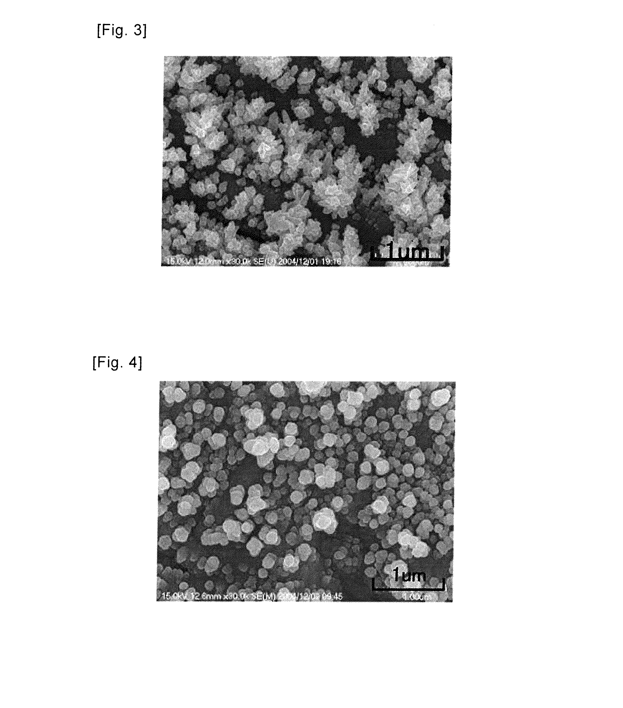
[0106]A primary particle layer (Cu) and a secondary particle layer (copper-cobalt-nickel alloy plating) were formed on rolled copper foil under the conditions and ranges shown below.

[0107]Bath compositions and the plating conditions used herein are as follows.

[Bath Compositions and Plating Conditions]

(A) Formation of a Primary Particle Layer (Cu Plating)

[0108]Solution composition: 15 g / L of copper, 75 g / L of sulfuric acid

[0109]Solution temperature: 35° C.

[0110]Current density: 2 to 58 A / dm2

[0111]Coulomb: 8 to 81 As / dm2

(B) Formation of a Secondary Particle Layer (Cu—Co—Ni Alloy Plating)

[0112]Solution composition: 15 g / L of copper, 8 g / L of nickel, 8 g / L of cobalt

[0113]pH: 2

[0114]Solution temperature: 40° C.

[0115]Current density: 24 to 31 A / dm2

[0116]Coulomb: 34 to 44 As / dm2


PUM

PropertyMeasurementUnit
Lengthaaaaaaaaaa
Lengthaaaaaaaaaa
Linear densityaaaaaaaaaa

Abstract

Disclosed is a copper foil for printed circuits prepared by forming a primary particle layer of copper on a surface of a copper foil, and then forming a secondary particle layer based on ternary alloy composed of copper, cobalt and nickel on the primary particle layer; in which the average particle size of the primary particle layer is 0.25 to 0.45 μm, and the average particle size of the secondary particles layer based on ternary alloy composed of copper, cobalt and nickel is 0.05 to 0.25 μm. Provided is a copper foil for printed circuits, in which powder fall from the copper foil can be reduced and the peeling strength and heat resistance can be improved by forming a primary particle layer of copper on a surface of a copper foil, and then forming a secondary particle layer based on copper-cobalt-nickel alloy plating on the primary particle layer.

Description

TECHNICAL FILED[0001]The present invention relates to a copper foil for printed circuits; more specifically relates to a copper foil for printed circuits, in which powder fall from the copper foil can be reduced and the peeling strength and heat resistance can be improved, prepared by forming a primary particle layer of copper on a surface of a copper foil, and then forming a secondary particle layer based on copper-cobalt-nickel alloy plating thereon.[0002]The copper foil for printed circuits of the present invention is particularly suitable for, for example, a fine-pattern printed circuit and a FPC (Flexible Printed Circuit) for magnetic heads.BACKGROUND ART[0003]Copper and copper alloy foils (hereinafter referred to as “copper foil”) have contributed significantly to the advances in the electric- and electronic-related industries and become essential, in particular, as materials for printed circuits. In general, a copper clad laminate is prepared by adhesively laminating a copper...

Claims


Application Information

Patent Timeline
IPC IPC(8): B32B15/01
CPCC25D1/04C25D3/38C25D3/562C25D3/58Y10T428/12028C25D7/0614C25D9/04H05K3/384C25D5/12C25D5/605H05K2203/0307C25D7/06H05K1/09H05K3/38C25D15/00H05K3/20
Inventor ARAI, HIDETAMIKI, ATSUSHI
Owner JX NIPPON MINING& METALS CORP
Learn More