Nanostructured arrays for radiation capture structures

a radiation capture and array technology, applied in the field of photon processing structures, can solve the problems of poor infrared absorption of crystalline silicon, use in solar photovoltaics, and difficulty in fabrication of these structures, and achieve the effect of improving at least one of photon capture and charge separation

Inactive Publication Date: 2013-01-17
MASSACHUSETTS INST OF TECH
View PDF3 Cites 11 Cited by
  • Summary
  • Abstract
  • Description
  • Claims
  • Application Information

AI Technical Summary

Benefits of technology

[0014]In other embodiments, the plurality of nanostructures (e.g., pyramids) can comprise a plurality of skewed nanostructures, which can act to enhance at least one of photon capture and charge separation relative to a plurality of non-skewed nanostructures which are similarly disposed. Such skewed nanostructures can be disposed in a lattice arrangement on the surface of the first doped layer (e.g., a triangle or square), which can help break the mirror symmetry of the nanostructures.

Problems solved by technology

Poor infrared absorption of crystalline silicon (c-Si) resulting from its indirect band gap poses a challenge to its use in solar photovoltaics.
However, fabrication of these structures can sometimes be difficult.

Method used


Image

  • Nanostructured arrays for radiation capture structures
  • Nanostructured arrays for radiation capture structures
  • Nanostructured arrays for radiation capture structures

Examples


Embodiment Construction

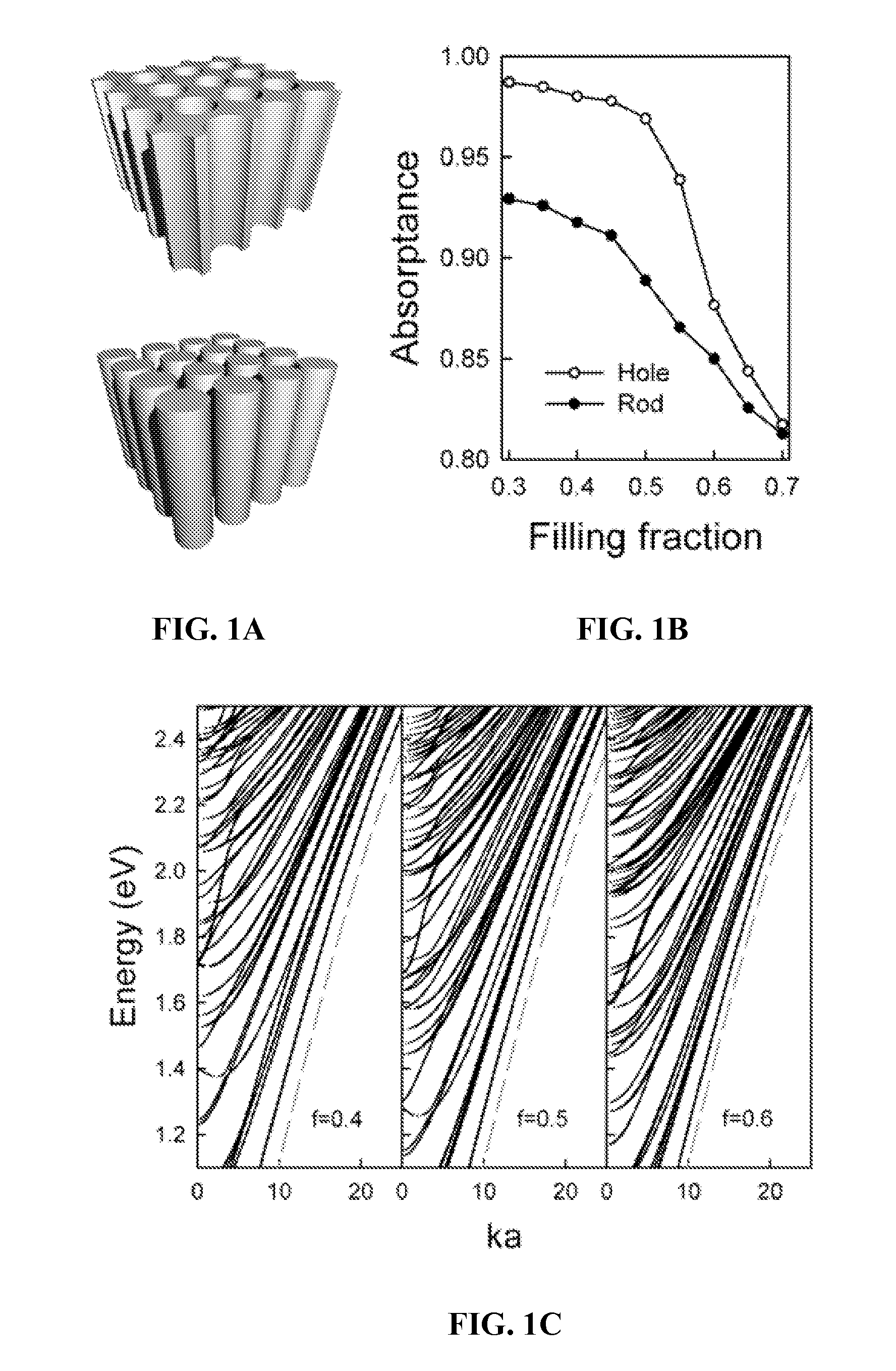
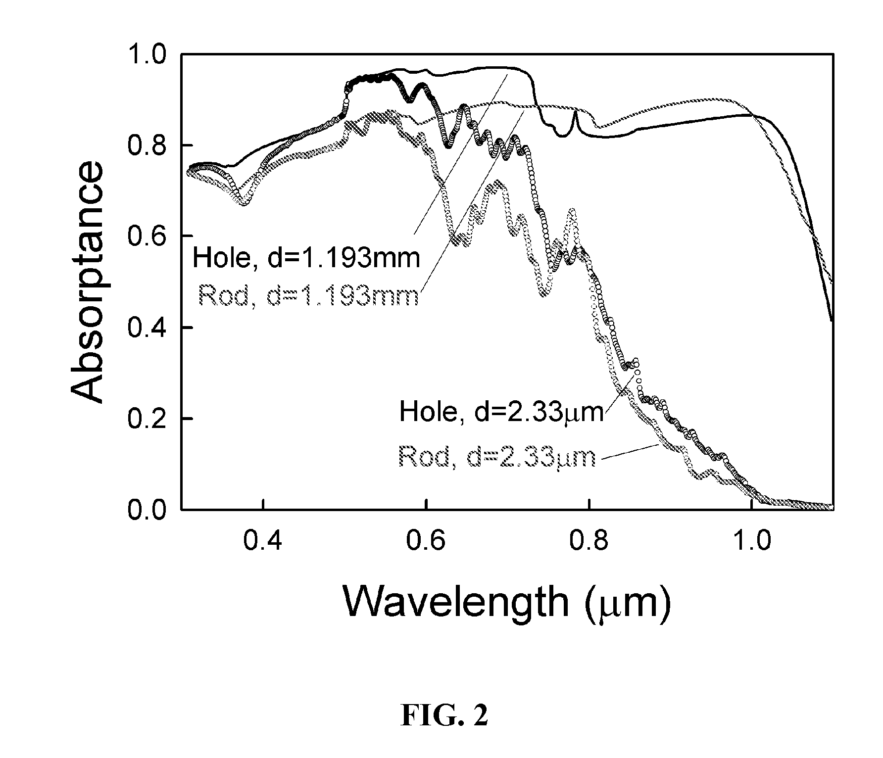
[0037]To evaluate the absorption performance of solar cells, we calculate the ultimate efficiency, η, which is defined as the efficiency of a photovoltaic cell as the temperature approaches 0° K when each photon with energy greater than the band gap produces one electron-hole pair:

η=∫0λgI(λ)A(λ)λλgλ∫0∞I(λ)λ,(1)

[0038]where I is the solar intensity per wavelength interval, A the absorptance, λ the wavelength, and λg the wavelength corresponding to the band gap. For the solar intensity, we use the Air Mass 1.5 spectrum. Equation (1) shows that, for a given absorption and solar radiation spectrum, λ / λg can be regarded as a weighting factor for integration. As the wavelength decreases from the band gap, the contribution of the absorbed solar energy to the ultimate efficiency decreases because the excess energy of photons above the band gap is wasted. Thus, while the solar Air Mass 1.5 spectrum peaks around 500 nm, the largest contribution to the ultimate efficiency of a c-Si solar cell c...


PUM


Abstract

Silicon nanohole arrays are disclosed as light absorbing structures for various devices such as solar photovoltaics. To obtain the same ultimate efficiency as a standard 300 micrometer crystalline silicon wafer, nanohole arrays require less silicon by mass. Moreover, calculations suggest that nanohole arrays may have efficiencies superior to nanorod arrays for practical thicknesses. With well-established fabrication techniques, nanohole arrays have great potential for efficient solar photovoltaics.

Description

FEDERALLY SPONSORED RESEARCH[0001]This invention was made with government support awarded by the National Science Foundation under Grant Number 00006178. The U.S. Government has certain rights in this invention.TECHNICAL FIELD[0002]The invention concerns photon processing structures and, in particular, light absorbing structures, which can be used in photovoltaics.BACKGROUND OF THE INVENTION[0003]Poor infrared absorption of crystalline silicon (c-Si) resulting from its indirect band gap poses a challenge to its use in solar photovoltaics. Currently, commercial solar cells have 200-300 micrometer c-Si active layers that absorb light efficiently. This thickness accounts for ˜40% of the total module cost and needs to be reduced to several micrometers. A thinner active layer has the added advantage of efficient charge-carrier transport. Thus, an effective technique for light trapping in thin active layers needs to be developed.[0004]While various structures employing randomly or periodi...

Claims


Application Information

Patent Timeline
Patent Type & Authority Applications(United States)
IPC IPC(8): H01L31/0248
CPCH01L31/02363Y02E10/50H01L31/035209
Inventor HAN, SANG EONMAVROKEFALOS, ANASTASSIOSBRANHAM, MATTHEW SANDERSCHEN, GANG
Owner MASSACHUSETTS INST OF TECH
Why Eureka
Try Eureka