

Patterning process and resist composition
- Summary
- Abstract
- Description
- Claims
- Application Information
AI Technical Summary
Benefits of technology
Problems solved by technology
Method used
Image

Examples
example
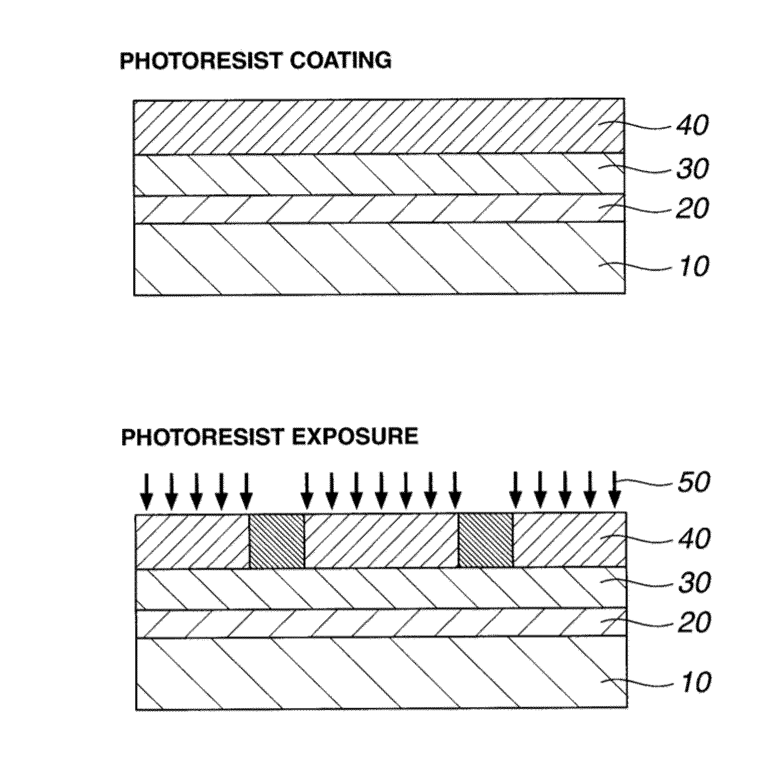
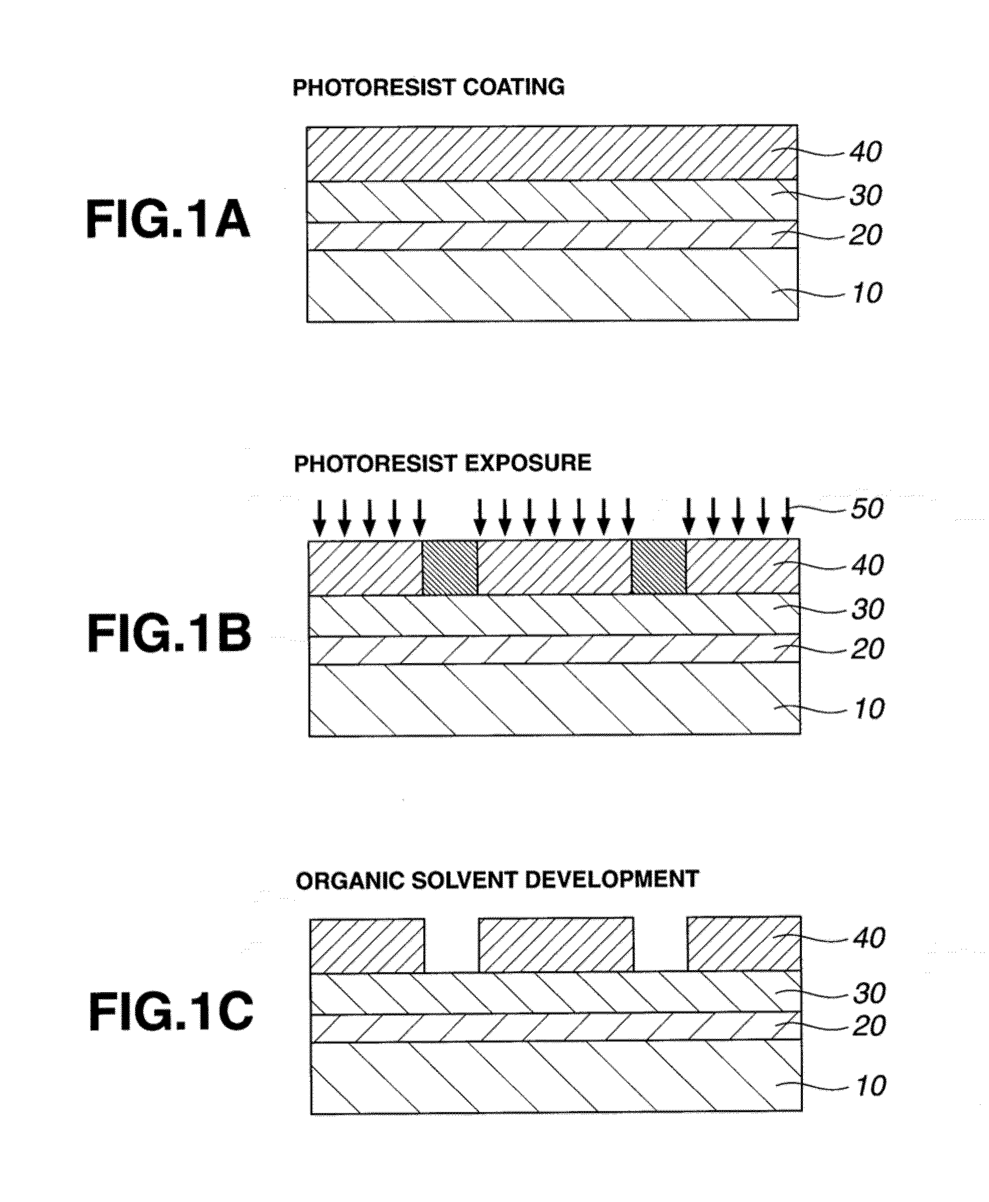
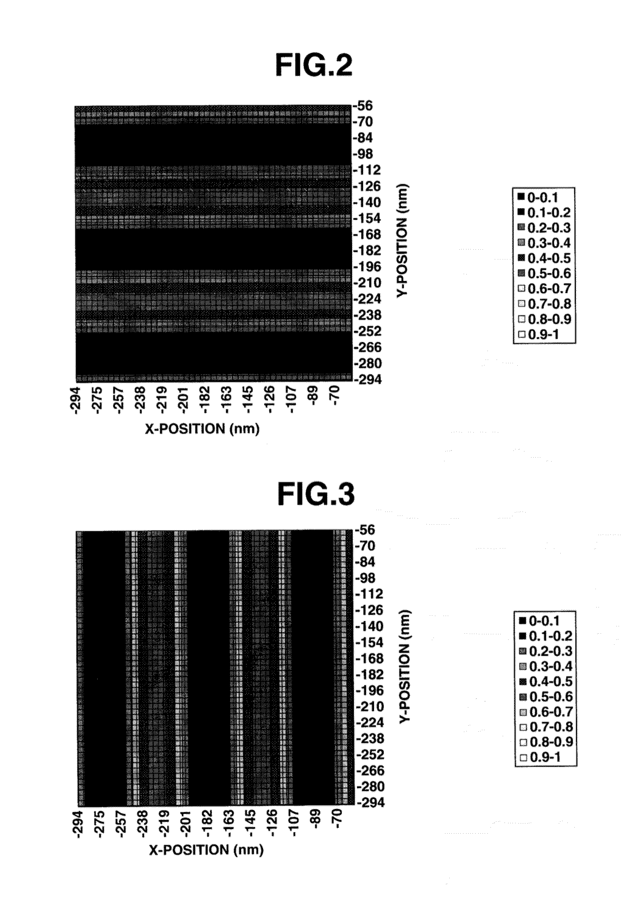
[0182]Examples of the invention are given below by way of illustration and not by way of limitation. The abbreviation “pbw” is parts by weight. For all polymers, Mw and Mn are determined by GPC versus polystyrene standards using tetrahydrofuran solvent. For measurement of the hole size of a pattern, a top-down scanning electron microscope (TDSEM) S-9380 (Hitachi High Technologies Corp.) was used.
synthesis example
[0183]Various polymers (Resist Polymers 1 to 16, Comparative Resist Polymer 1, and Blending Resist Polymers 1, 2) for use in resist compositions were prepared by combining suitable monomers, effecting copolymerization reaction in tetrahydrofuran solvent, pouring into methanol for crystallization, repeatedly washing with hexane, isolation, and drying. The polymers were analyzed by 1H-NMR to determine their composition and by GPC to determine Mw and dispersity Mw / Mn.
PUM
 Abstract
Description
Claims
Application Information