Electrodeposited Nano-Twins Copper Layer and Method of Fabricating the Same

Active Publication Date: 2013-05-16
NAT CHIAO TUNG UNIV
View PDF2 Cites 28 Cited by
  • Summary
  • Abstract
  • Description
  • Claims
  • Application Information

AI Technical Summary

Benefits of technology

[0058]The figures presented herein are simplified diagrams showing examples of the current invention. It must be understood that the figures are only illustrative of the associated elements of the current invention, and are

Problems solved by technology

In terms of electrical performance of microelectronic devices, electromigration has become a critical reliability issue of Cu wires.
The atoms move along the direction of the moving electrons and result in electro-migration damage.
But the twins material prepared by these known technologies illustrated above can only obtain miniscaled and irregular nano-twins, and suffer high production cost.
In addition, PVD cannot fill Cu in trenches or vias with a high-aspect ratio.
Hence, these known methods are not widely applied in mass production of semiconductor and electronic products.
In other words, these methods still cannot be applied in industrial mass production.
In addition, because physical vapor phase deposition inherently cannot plate a concaved trough of a high aspect ratio well and deposition duration is long, neither structure nor its preparative method is applicable for use in copper interconnects, through silicon via, or under-bump metallization (UBM), etc.
One drawback of the known technology comes from the fact that the size of produced crystal grains is too small, the twins cop

Method used


Image

  • Electrodeposited Nano-Twins Copper Layer and Method of Fabricating the Same
  • Electrodeposited Nano-Twins Copper Layer and Method of Fabricating the Same
  • Electrodeposited Nano-Twins Copper Layer and Method of Fabricating the Same

Examples


example 1

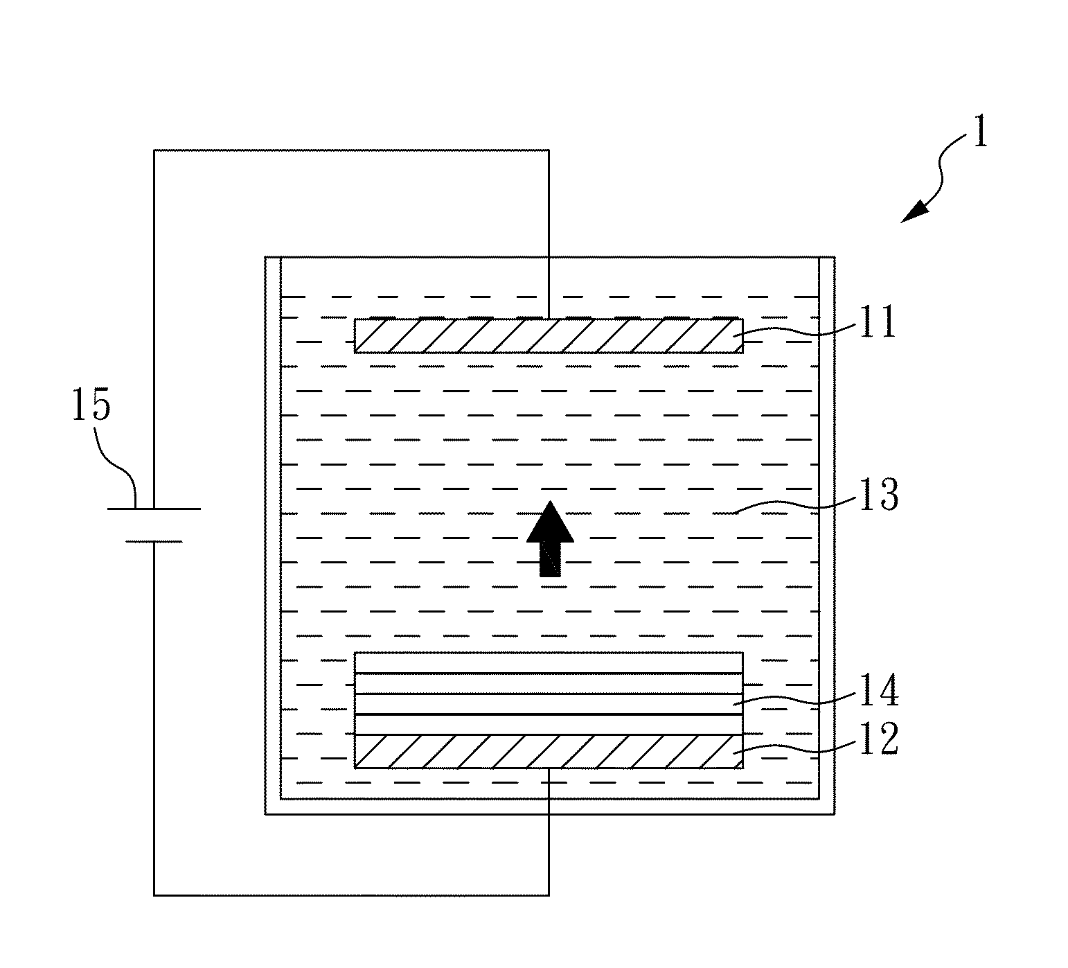
[0059]An electrodepositing device 1 as shown in FIG. 1 is provided, the electrodepositing device 1 comprises an anode 11, a cathode 12, which are immersed in the plating solution 13 and are each connected to a direct current electrical power supply source 15 (Keithley 2400 is used herein). In the present case, the anode 11 is made from a material including metal copper, phosphorus copper or inert anode (for example, titanium-plated platinum); cathode 12 is made from a material including silicon substrate having its surface plated by copper seed layer, and can be made from a material selected from a group consisting of glass substrate having its surface plated by conductive layer and seed layer, conductive layer and seed layer plated surface glass substrate, quartz substrate, metal substrate, plastic substrate, or printed circuit board etc. The plating solution 13 comprises copper sulfate (copper ion concentration being 20-60 g / L), chloride anion (concentration being 10-100 ppm), and...

example 2

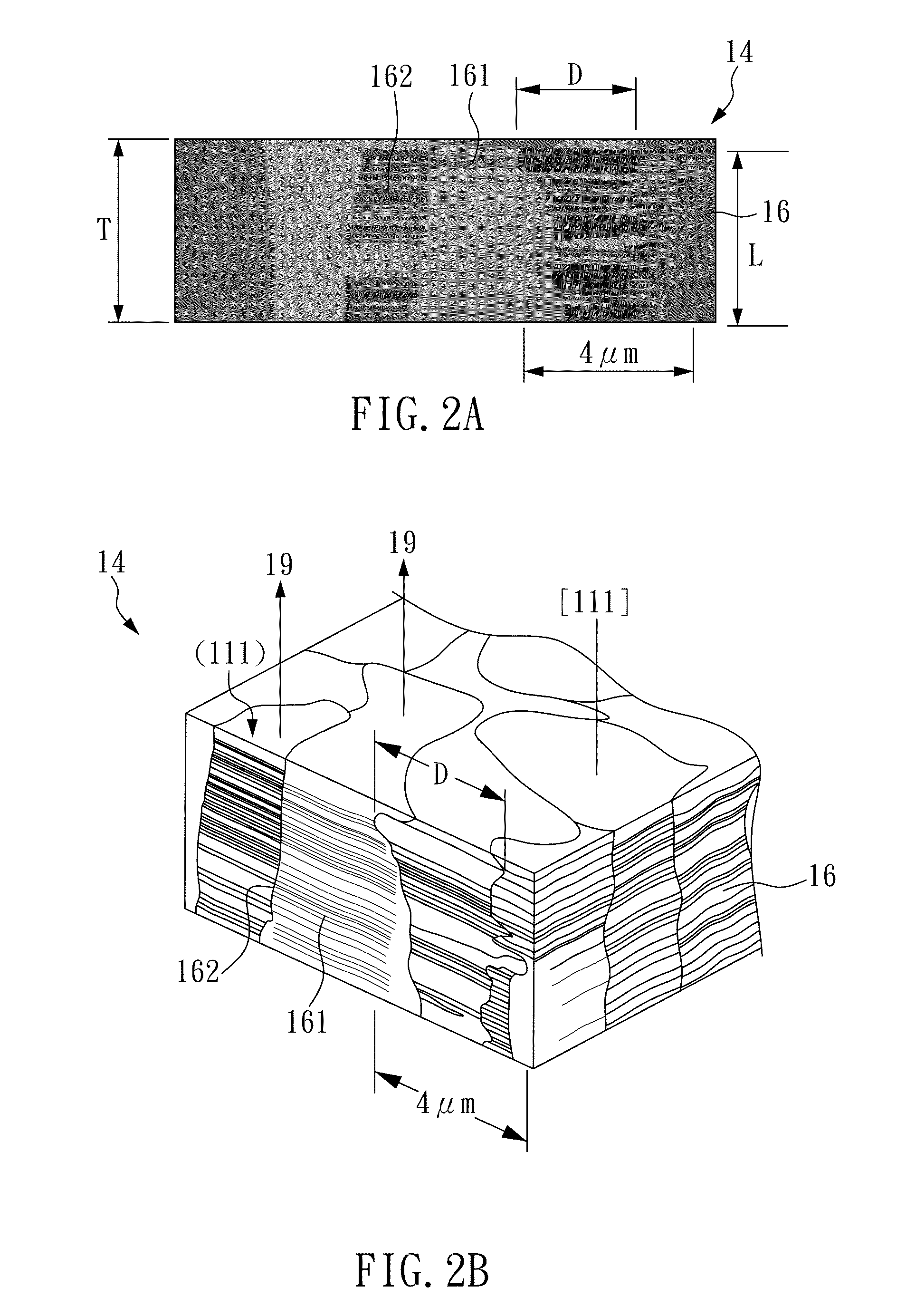
[0067]The combination of electrodepositing device and plating solution of the present example is the same as in Example 1, but pulse electrodeposition is used for plating instead of direct current power supply source. Silicon chip or solution is subject to rotation at a rate of about 0 to 1500 rpm. Ton / Toff is kept below 0.1 / 0.5 (sec), electric current density is kept at 50 mA / cm2, and twins copper is grown (plating 6000 cycles) from cathode moving toward the direction pointed by the arrow (as shown in FIG. 1). [111] plane of the twins is perpendicular to the orientation of electric field, and twins copper is grown at a rate of 0.183 μm / min. The fully grown twins copper comprises a plurality of columnar crystal grains; the columnar crystal grain has a plurality of layer-shaped nano-twins copper, and the thickness of the nano-twins copper layer obtained after electrodeposition is about 10 μm.

[0068]FIG. 9 is a cross-sectional focused ion beam (FIB) photo of the nano-twins copper metal...

example 3

[0070]The plating solution and method of the present example is the same as Example 1, but is different in an aspect that the current example has wire channel prepared by a semiconductor manufacturing process on the substrate surface, the micro through holes of the aspect ratio of 1:3, and that the nano-twins copper metal layer uses electrodeposition to fill holes and in turn forms interconnect.


PUM

PropertyMeasurementUnit
Fractionaaaaaaaaaa
Fractionaaaaaaaaaa
Fractionaaaaaaaaaa

Abstract

An electrodeposited nano-twins copper layer, a method of fabricating the same, and a substrate comprising the same are disclosed. According to the present invention, at least 50% in volume of the electrodeposited nano-twins copper layer comprises plural grains adjacent to each other, wherein the said grains are made of stacked twins, the angle of the stacking directions of the nano-twins between one grain and the neighboring grain is between 0 to 20 degrees. The electrodeposited nano-twins copper layer of the present invention is highly reliable with excellent electro-migration resistance, hardness, and Young's modulus. Its manufacturing method is also fully compatible to semiconductor process.

Description

CROSS-REFERENCE TO RELATED APPLICATIONS[0001]This present application relies on Taiwanese Patent Application No. 100141898 filed on Nov. 16, 2011. The abovementioned foreign application is herein incorporated by reference in their entirety.BACKGROUND OF THE INVENTION[0002]1. Field of the Invention[0003]The present invention relates to a method for preparing electrodeposited nano-twins copper layer and the nano-twins copper layer prepared by the same, more particularly, to a method for preparing a nano-twins copper layer having a plurality of [111] surfaces on its surface and the nano-twins copper layer thereof.[0004]2. Description of Related Art[0005]Mechanical strength of metallic material increases generally when the size of the crystal grain is reduced to a nanoscale level. Some nano-scale levels of thin metal films can even have particular mechanical properties such—Young's coefficient. As a result, twins metal having nanoscale crystalline properties will be suitable for applica...

Claims


Application Information

Patent Timeline
IPC IPC(8): C30B7/12C30B29/02C30B29/60
CPCC30B7/12C30B29/605C30B29/02C25D3/38C25D5/08Y10T428/12674H01L21/2885H01L21/76898H01L21/76877C25D21/10Y10T428/12903C25D5/18C25D5/617
Inventor CHEN, CHIHTU, KING-NINGLIU, TAOCHI
Owner NAT CHIAO TUNG UNIV
Why Eureka
Try Eureka