Laser micro/nano processing system and method

a technology of laser micro/nano and processing system, which is applied in the field of laser micro/nano processing, can solve the problems of difficult conventional technologies to obtain micro/nano devices with complicated structures, limited processing resolution, and inapplicability to other materials, so as to achieve precise control of fabrication resolution and accuracy, and the range of materials applicable to laser micro/nano fabrication may be extended.

Active Publication Date: 2013-07-18
TECHNICAL INST OF PHYSICS & CHEMISTRY - CHINESE ACAD OF SCI
View PDF3 Cites 32 Cited by
  • Summary
  • Abstract
  • Description
  • Claims
  • Application Information

AI Technical Summary

Benefits of technology

[0008]One object of the present invention is to provide a laser micro / nano fabrication method and fabrication system, by which the fabrication resolution and accuracy can be precisely controlled. According to the invention, by selecting two laser beams to have the wavelengths matching the characteristics of the photosensitive material to be processed and irradiating selected laser beams, the range of the materials applicable to laser micro / nano fabrication may be extended and the accuracy of the laser micro / nano fabrication will be improved.

Problems solved by technology

Since the conventional single-photon lithography is achieved on basis of its planar nature, the processing resolution is restricted by the optical diffraction limit.
Meanwhile it is difficult for the conventional technologies to obtain a micro / nano device with complicated structures.
However, the above mentioned methods are only be applicable to the materials that can be excited by laser and their excited state may be depleted, and are not applicable to other materials.
However, currently fabrication of the metal micro / nano structure with femtosecond laser may achieve the resolution more than one hundred nanos, it is difficult to achieve a metal structure of nano-scale.
Therefore, the conventional femtosecond laser technology is limited to process the photosensitive material formed on the glass substrate.

Method used


Image

  • Laser micro/nano processing system and method
  • Laser micro/nano processing system and method
  • Laser micro/nano processing system and method

Examples


embodiment 1

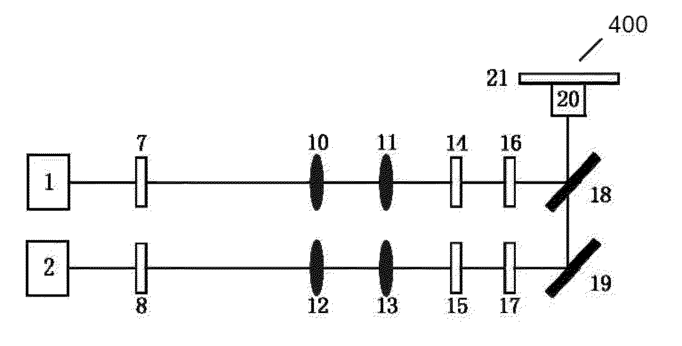
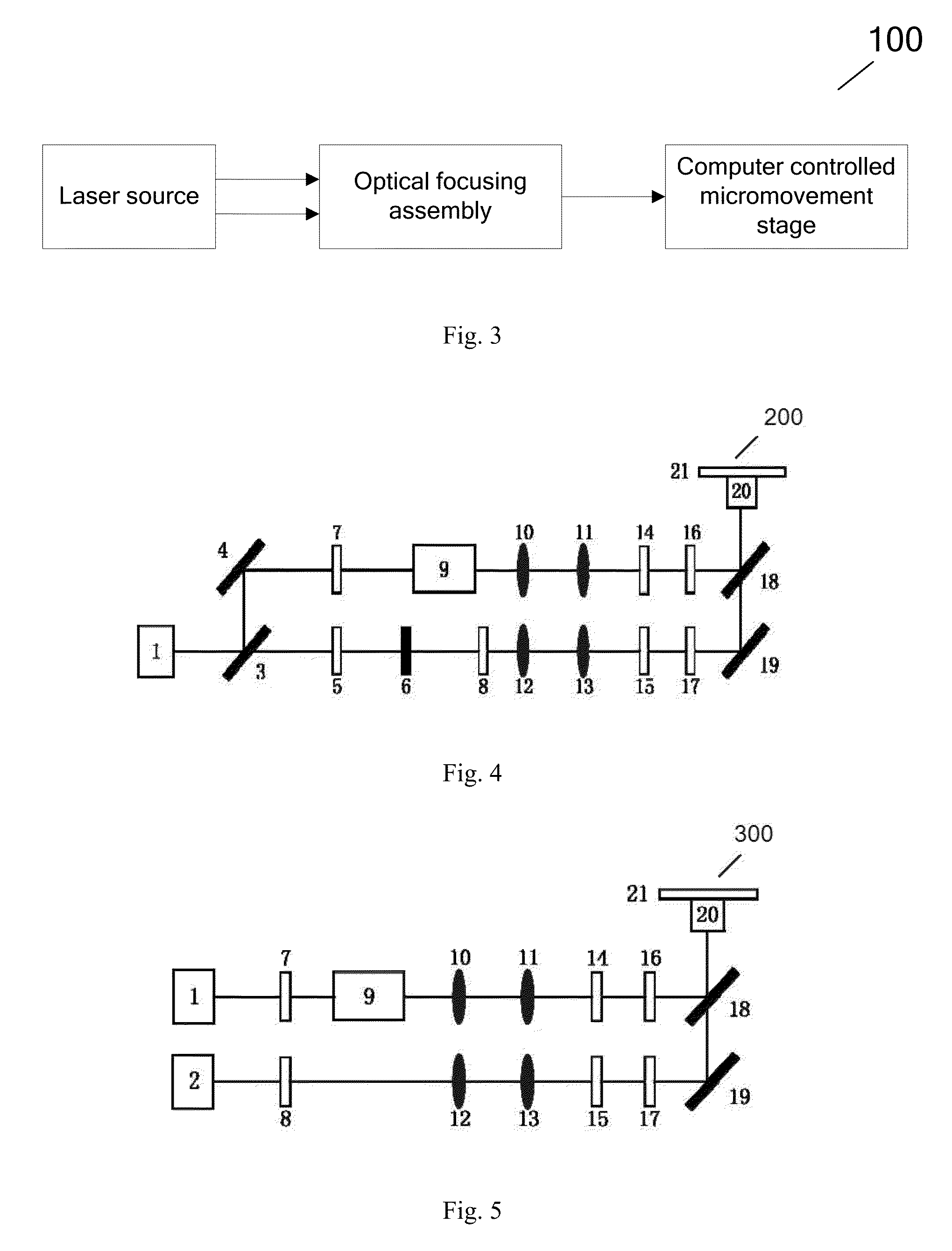
[0110]FIG. 4 illustrates a layout of the laser micro / nano fabrication system according to Embodiment 1 of the invention. The laser micro / nano fabrication system 200 includes a laser 1, a half reflecting and half transmitting mirror 3, a frequency multiplier 5, for example a frequency-doubling crystal, an optical delay assembly 9, an optical focusing assembly and a movement stage 21. The laser 1 outputs the pulsed laser beam having a pulse width in range of nanosecond to femtosecond. The half reflecting and half transmitting mirror 3 is placed in the output light path of the laser 1 for forming a transmitting light and a reflecting light. The frequency doubling crystal 5 and a filter 6 are placed in this order along the transmission light path. The filter 6 filters the frequency-doubled laser beam, and in the output of the filter, the ratio of the energy of the frequency-doubled laser beam is not less than 99.5% of the total energy of the laser beam output from the filter. Following ...

example 1

[0126]The following will describe the specific steps by example of preparation of linear array structure in the commercial SCR500 photoresist applied on the glass substrate using the laser micro / nano fabrication system of the invention.

[0127]The system used in this example is the laser micro / nano fabrication system 200 shown in FIG. 4. The laser 1 is a femtosecond Ti: sapphire laser, which generates a laser beam having wavelength of 800 nm, pulse width of 100 fs, pulse repetition rate of 82 MHz, diameter of 1.8 mm and being in linear polarization state. In the output light path of the laser 1, there is a half reflecting and half transmitting mirror 3 made of e.g. glass BK7, with the ratio of transmission / reflection of e.g. 7:3, for forming the transmissive light and reflective light. The frequency multiplier 5 on the transmission path includes for example a 1-mm type I BBO frequency-doubling crystal 5 and a interference filter 6 placed in this order along the main axis of the light ...

example 2

[0130]The specific steps will be described with reference to FIG. 4 by example of preparation of a suspended line structure in the commercial SCR500 photoresist applied on the glass substrate using the laser micro / nano fabrication system and method of the invention.

[0131]Except for the delay assembly 9, the other elements used in this example are as the same as the elements used in Example 1. In the reflection path of the half transmitting and half reflecting mirror 3, a reflecting mirror 4 made of glass BK7 for example, is placed along the main axis to keep the reflection path to be parallel to another path. Following the mirror 3, the optical delay assembly 9 is provided including a one-dimensional micromovement platform 22 and two right-angle prisms made of glass BK7 27 and 28, shown in FIG. 7. Then a 35-mm lens 10 and a 150-nm lens 11 are placed for expanding the fundamental frequency laser beam, and a 800-nm half-wave plate 14 is placed with its optical axis being consistent wi...


PUM

PropertyMeasurementUnit
wavelengthaaaaaaaaaa
FWHMaaaaaaaaaa

Abstract

A laser micro/nano processing system (100, 200, 300, 400) comprises: a laser light source used to provide a first laser beam having a first wavelength and a second laser beam having a second wavelength different from the first wavelength, with the pulse width of the first laser beam being in the range from a nanosecond to a femtosecond; an optical focusing assembly used to focus the first laser beam and the second laser beam to the same focal point; and a micro mobile platform (21) controlled by a computer. Also disclosed are a method for micro/nano-processing photosensitive materials with a laser and a method for fabricating a device with a micro/nano structure using laser two-photon direct writing technology. In the system and methods, spatial and temporal overlapping of two laser beams is utilized, so as to obtain a micro/nano structure with a processing resolution higher than that of a single laser beam, using an average power lower than that of a single laser beam.

Description

FIELD OF THE INVENTION[0001]The present invention relates to laser micro / nano processing, and more particularly to a laser micro / nano processing system and processing method, which precisely controls the processing resolution and accuracy.BACKGROUND OF THE INVENTION[0002]In the past 50 years, lithography has been dominated the micro / nano processing technology. Since the conventional single-photon lithography is achieved on basis of its planar nature, the processing resolution is restricted by the optical diffraction limit. In order to achieve a higher resolution, the lithography uses the wavelength of the laser output from the light source from infrared laser to DUV KrF laser (248 nm) and ArF laser (193 nm), with processing method from the traditional laser lithography, to X-ray lithography, electron-beam lithography, ion-beam lithography, nanopattern transfer, and so on. These technologies may prepare two-dimensional or quasi-three-dimensional structures by plane method, probe meth...

Claims


Application Information

Patent Timeline
Patent Type & Authority Applications(United States)
IPC IPC(8): B81C1/00B23K26/08B23K26/06H01L21/02
CPCB23K26/0613B23K26/0635B23K26/0676B23K26/0639G03F7/70375B81C1/00428H01L21/02107G03F7/2053B23K26/083B23K26/0624B23K26/048B23K26/0643B23K26/0648B23K26/064
Inventor DUAN, XUANMINGCHEN, SHUCAO, HONGZHONGDONG, XIANZIZHAO, ZHENSHENG
Owner TECHNICAL INST OF PHYSICS & CHEMISTRY - CHINESE ACAD OF SCI
Why Eureka
Try Eureka