Nano mosfet with trench bottom oxide shielded and third dimensional p-body contact

Active Publication Date: 2013-08-08
ALPHA & OMEGA SEMICON INC
View PDF11 Cites 78 Cited by
  • Summary
  • Abstract
  • Description
  • Claims
  • Application Information

AI Technical Summary

Benefits of technology

[0051]In this Schottky-Source Nano MOSFET device, Schottky contact allows lower P-body dose, and the P-shield prevent P-body punch through, which enables to achieve low threshold

Problems solved by technology

However, thinning the gate oxide layer to enhance the current drive renders the gate oxide layer more easily affected by the punch-through effect.
Conventional technologies to configure and manufacture high voltage semiconductor power devices are still confronted with difficulties and limitations to further improve the performances due to different tradeoffs.
However, a drawback of such a technique is that thermal oxidation increases the thermal budget required in the process.
However, the SGT MOSFET structure presents challenges in forming the dielectric isolation between the shield electrode and gate electrode, unclamped inductive switching

Method used


Image

  • Nano mosfet with trench bottom oxide shielded and third dimensional p-body contact
  • Nano mosfet with trench bottom oxide shielded and third dimensional p-body contact
  • Nano mosfet with trench bottom oxide shielded and third dimensional p-body contact

Examples


second embodiment

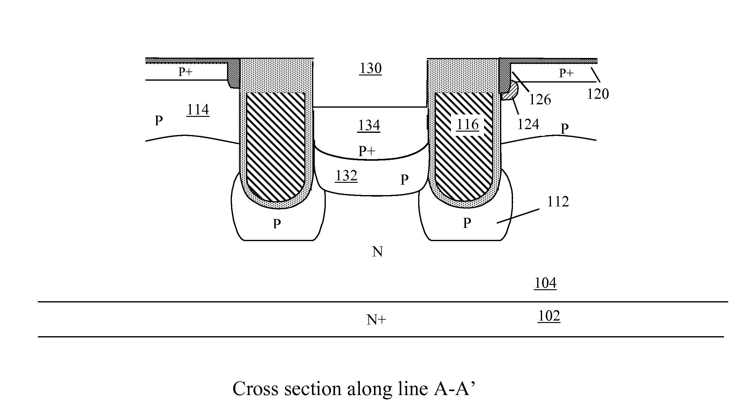
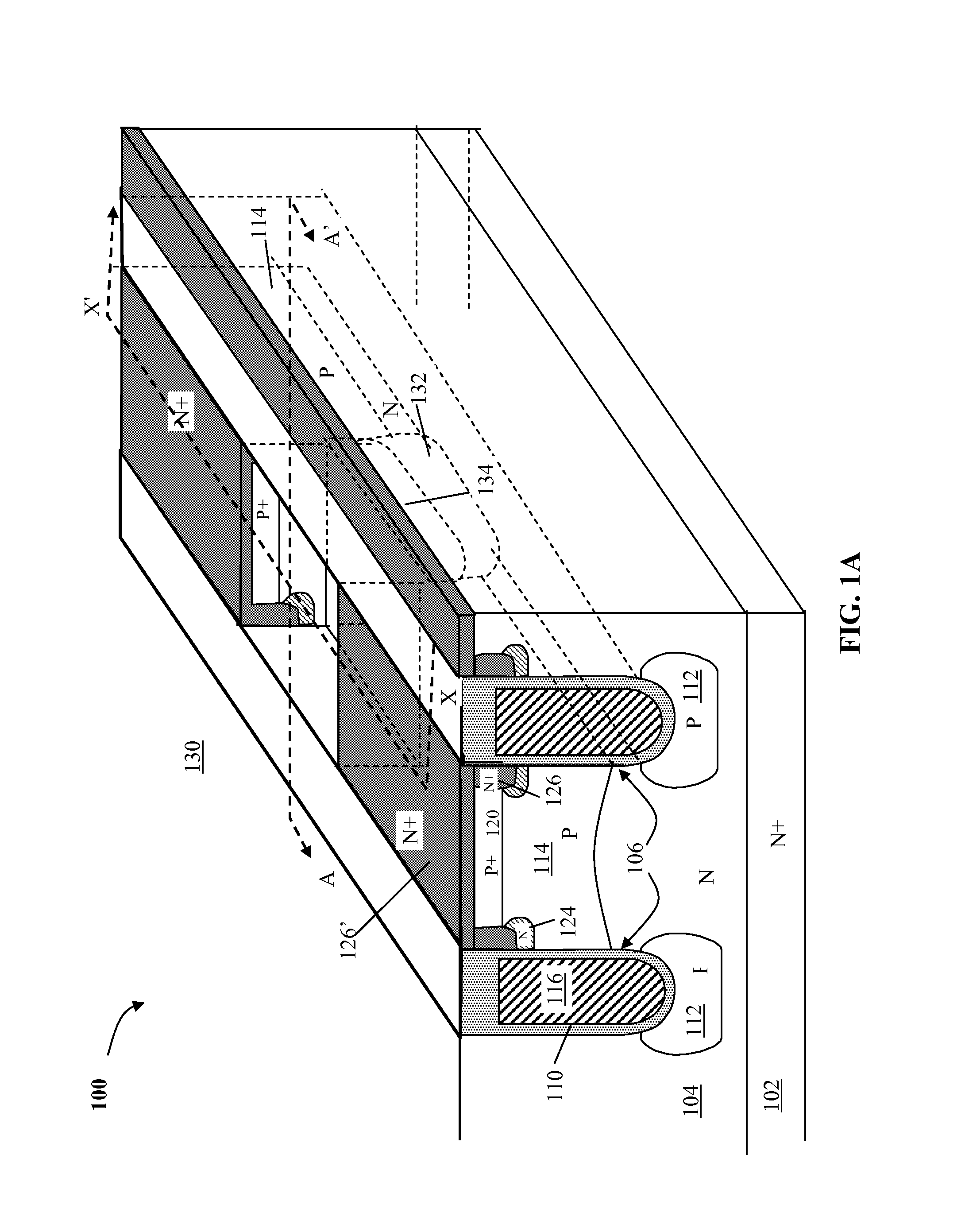
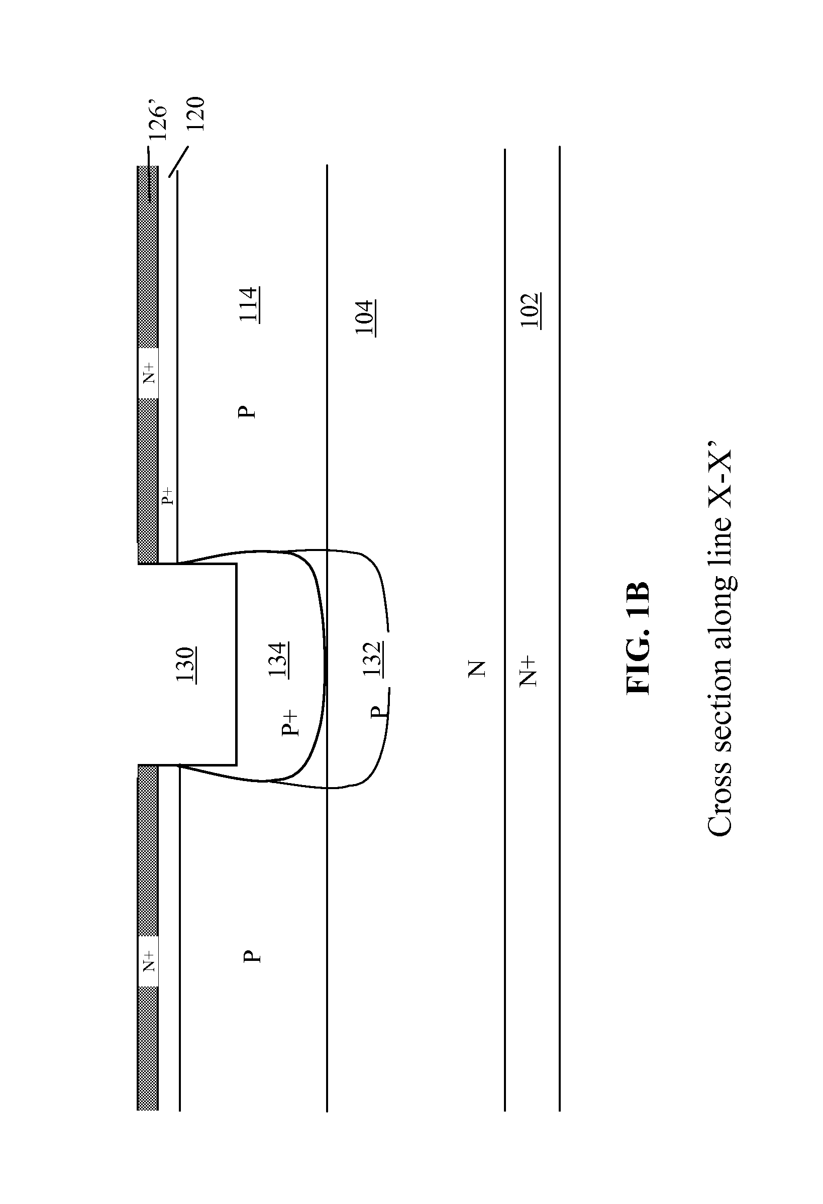
[0040]The nano-MOSFET with third dimensional deep P+ contact of the type depicted in FIG. 1A can also be applied for a nano-MOSFET with a thick bottom oxide (TBO). FIG. 3A is a three-dimensional schematic diagram of a nano-MOSFET with third dimensional deep P+ contact with TBO 300 according to the present invention. The device 300 is similar to the device 100 except that, a thick bottom oxide (TBO) 312 is formed inside and at the bottom of each trench 106, under the gate electrode 116, for shielding the gate electrode 116 therefore shielding implant under the gate trench is not needed.

[0041]As a result the deep P implant region 132 below the third dimensional deep P+ contact region 134 becomes optional as the connection to the deep P implant region 112 is needed.

[0042]FIG. 3B is a cross-sectional schematic diagram of the device 300 after source and gate metal are formed. The structure of the device 300 in FIG. 3B is similar to the structure of the device shown in FIG. 2P, except tha...

third embodiment

[0044]Nano MOSFET technology can be further ruggedized by replacing N+ source region with Schottky Contact. FIGS. 4A-4N are cross-sectional schematic diagrams illustrating a process of manufacturing a Schottky-Source Nano MOSFET with third dimensional deep P+ contact and deep P implant for shielding gate electrode according to the present invention.

[0045]As seen in FIG. 4A, the process may begin by forming an initial layer of insulator, e.g., oxide 208, on the N-type semiconductor substrate 204, a lower portion 202 of which is heavily doped with the N-dopant to act as a drain. A first photoresist (not shown), which is a trench mask, may be formed on the oxide 208 and then developed followed by patterning the oxide 208 to form the openings in the oxide 208. The trench mask is removed and gate trenches 206, including contact gate trench 206-1, dummy gate trench 206-2, active gate trenches 206-3 and 206-4 as shown, may then be etched in the semiconductor substrate 204 through the openi...

fourth embodiment

[0052]The Schottky-Source Nano MOSFET configuration shown in FIG. 4N can be applied for Nano MOSFET with a thick bottom oxide (TBO). FIG. 5 is a cross-sectional schematic diagram illustrating a Schottky-Source Nano MOSFET device with third dimensional deep P+ contact and thick bottom oxide 512 according to the present invention. The device structure shown in FIG. 5 is similar to the structure shown in FIG. 4N except that the deep P implant regions 212 is replaced with thick bottom oxide 512 for shielding the gate electrode 216. As such, the process of making this device is similar to the process shown in FIGS. 4A-4N with the step of P-type dopant through the trench 206 in FIG. 4B being skipped.

[0053]In addition, the Schottky-Source Nano MOSFET configuration shown in FIG. 4N can also be implemented for devices having the Nano SGT MOSFET configuration with a gate structure similar to that in FIG. 9.

[0054]FIG. 6 is a cross-section view illustrating a termination area of the Nano MOSFET...


PUM


Abstract

A semiconductor power device may include a lightly doped layer formed on a heavily doped layer. One or more devices are formed in the lightly doped layer. Each device may include a body region, a source region, and one or more gate electrodes formed in corresponding trenches in the lightly doped region. Each of the trenches has a depth in a first dimension, a width in a second dimension and a length in a third dimension. The body region is of opposite conductivity type to the lightly and heavily doped layers. The source region is formed proximate the upper surface. One or more deep contacts are formed at one or more locations along the third dimension proximate one or more of the trenches. The contacts extend in the first direction from the upper surface into the lightly doped layer and are in electrical contact with the source region.

Description

FIELD OF THE INVENTION[0001]This invention relates in general to semiconductor power field effect transistor devices and in particular relates to new configurations and methods for manufacturing improved nano trench Metal-Oxide Semiconductor Field Effect Transistor (MOSFET) devices.BACKGROUND OF THE INVENTIONS[0002]Nowadays, trench-type MOSFET devices are broadly used as power witches in electronic appliance. The difference between the trench-type MOSFET device and the traditional MOSFET device is that the gate structure of the former is formed in a trench to minimize the area of the MOSFET device, thereby enhancing the density of the MOSFET device and reducing the on-resistance. However, thinning the gate oxide layer to enhance the current drive renders the gate oxide layer more easily affected by the punch-through effect.[0003]Conventional technologies to configure and manufacture high voltage semiconductor power devices are still confronted with difficulties and limitations to fu...

Claims


Application Information

Patent Timeline
IPC IPC(8): H01L29/78H01L21/336
CPCH01L21/26586H01L29/407H01L29/41766H01L29/42368H01L29/456H01L29/66727H01L29/1095H01L29/7811H01L29/7813H01L29/0623H01L29/0626H01L29/086H01L29/0869H01L29/66734H01L27/088H01L29/0865H01L29/404H01L29/4236
Inventor YILMAZ, HAMZANG, DANIELCALAFUT, DANIELBOBDE, MADHURBHALLA, ANUPPAN, JILEE, YEEHENGKIM, JONGOH
Owner ALPHA & OMEGA SEMICON INC
Why Eureka
Try Eureka