Electroanalytical sensor based on nanocrystalline diamond electrodes and microelectrode arrays

Active Publication Date: 2013-08-22
JOHN CRANE INC
View PDF2 Cites 22 Cited by
  • Summary
  • Abstract
  • Description
  • Claims
  • Application Information

AI Technical Summary

Benefits of technology

[0026]A higher voltage is required for detection of small molecules, and the microelectrode array comprising UNCD microlectrodes having a resistivity of >0.05 Ωcm and a surface roughness of <20 nm Ra provides a low-noise microelectrode array that can be used at a higher peak signal voltage, i.e. a peak signal amplitude of >25 mV, >50 mV or up to 100 mV to provide sufficient sensitivity to detect smaller target molecules.
[0027]For a given geometric area, UNCD and NCD surfaces exhibit lower background currents, i.e. at least 10× lower, and thus exhibit improved

Problems solved by technology

However, commercial development of such sensors has been hindered by issues such as poor signal to noise ratios, resulting in difficulty in interpreting a change in impedance on antigen binding and poor signal reproducibility as a result of surface fouling and non-specific binding.
When modifying electrode surfaces with recognition molecules using covalent immobilization chemistries, most surfaces (Pt, Au, silicon and non-conductive silica glass slides) are not hydrolytically stable and thus oxidize the recognition molecules that are critical to detect targets selectively.
For metals with high electrica

Method used


Image

  • Electroanalytical sensor based on nanocrystalline diamond electrodes and microelectrode arrays
  • Electroanalytical sensor based on nanocrystalline diamond electrodes and microelectrode arrays
  • Electroanalytical sensor based on nanocrystalline diamond electrodes and microelectrode arrays

Examples


Embodiment Construction

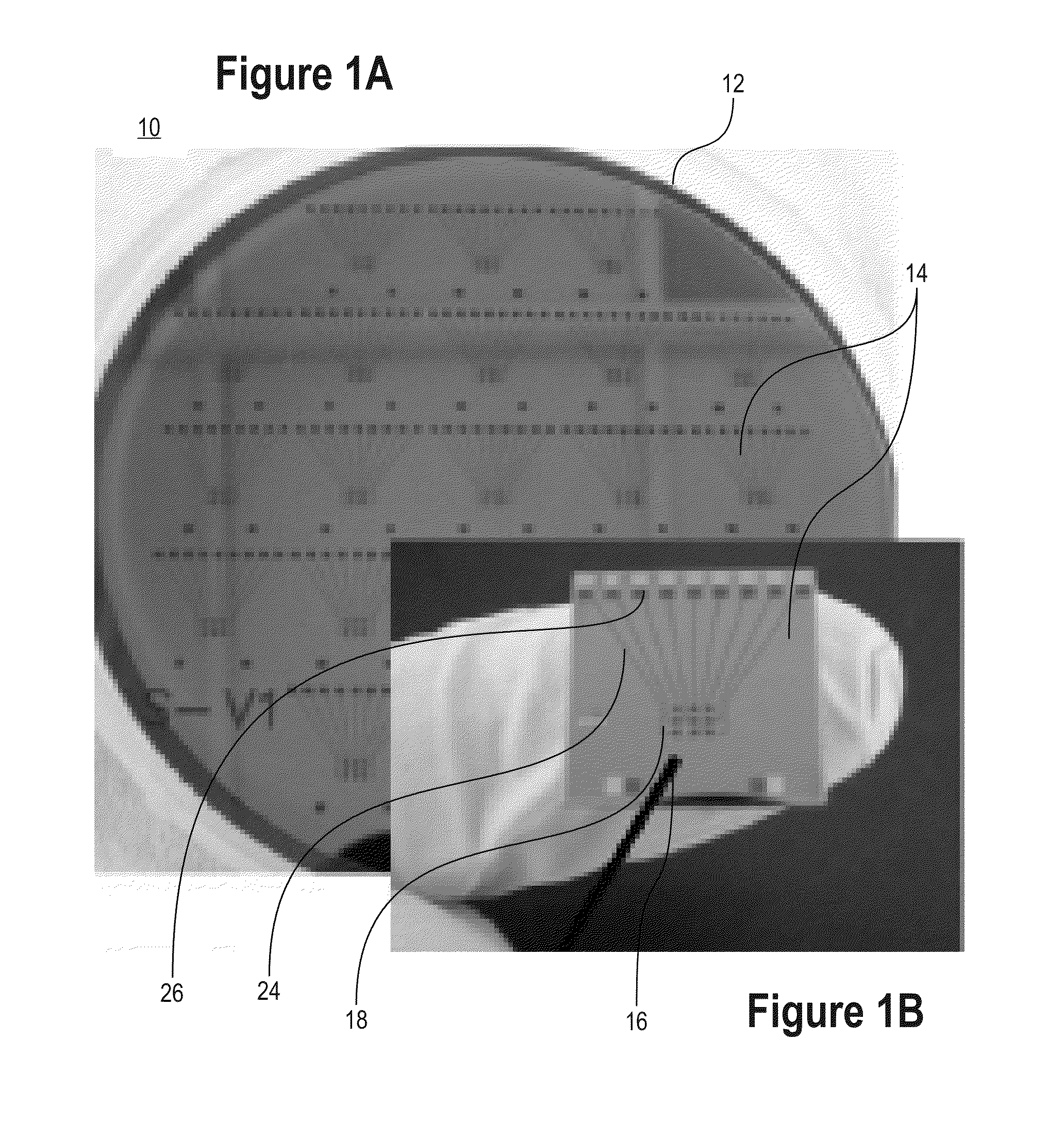
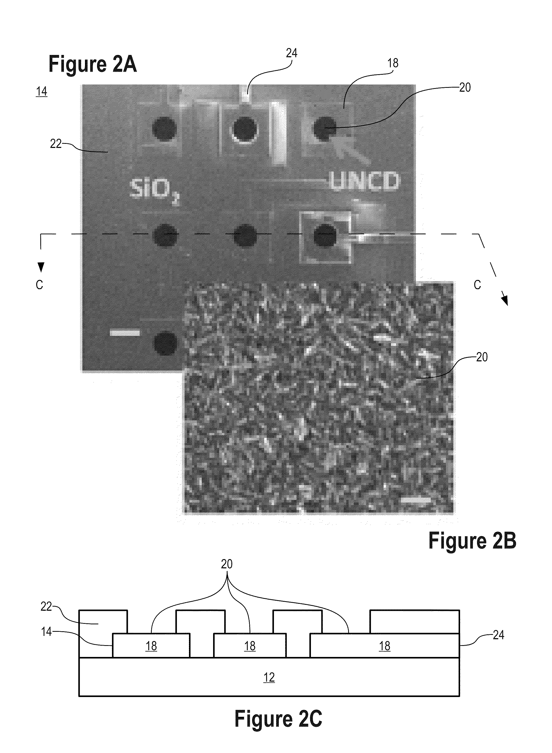
[0046]FIG. 1A shows an optical image of a substrate comprising a 4 inch wafer 10 comprising a silicon substrate 12 having fabricated thereon a plurality of chips or die 14, each comprising a 3×3 UNCD microelectrode array (MEA) 16, according to an embodiment of the present invention. In this example, as shown enlarged in FIG. 1B, each microelectrode 18 has an active area 200-μm in diameter and conductive traces 24 are provided to individually connect each microelectrode to a respective contact pad 26. FIG. 2A shows a SEM image of part of one of the chips 14 showing an enlarged view of the nine individually addressable microelectrodes 18 of the MEA 16, with the overlying passivation layer 22 having apertures over each electrode. A SEM image showing the ultrasmooth UNCD surface morphology is shown in FIG. 2B.

[0047]As shown in FIG. 2C, which shows a cross-section C-C through the MEA 16 shown in FIG. 2A, the MEA is fabricated on a silicon substrate 12 on which is formed a dielectric laye...


PUM

PropertyMeasurementUnit
Thicknessaaaaaaaaaa
Diameteraaaaaaaaaa
Diameteraaaaaaaaaa

Abstract

A diamond electrode and a diamond microelectrode array for biosensors and electroanalytical applications, such as electrochemical impedance spectroscopy (EIS), are disclosed. The electrode comprises a layer of ultra-smooth conductive nanocrystalline diamond (NCD) having a resistivity of >0.05 Ωcm and a surface roughness of <20 nm Ra. Preferably, the diamond layer comprises boron or nitrogen-doped ultrananocrystalline diamond (UNCD) having an average grain size <10 nm and a surface roughness <10 nm Ra. It may be patterned to define a microelectrode array with a plurality of individually addressable electrodes, each having a diameter in the range from 100 nm to 100 μm. The surface of each microelectrode is hydrogen-terminated before bio-functionalization, i.e. modifying with sensing molecules for detection of a specific biological or chemical target and coating with a blocker for reducing non-specific binding. These diamond electrodes exhibited substantial increases in sensitivity, selectivity and signal reproducibility, e.g. for detection of E. coli K12 using EIS.

Description

CROSS-REFERENCE TO RELATED APPLICATIONS[0001]This application claims priority from U.S. provisional patent application Ser. No. 61 / 602,032, entitled “A Highly Robust Electroanalytical Platform Based on Nanocrystalline Diamond Arrays” filed Feb. 22, 2012. This application is incorporated herein by reference, in its entirety.TECHNICAL FIELD[0002]This invention relates to electrodes and microelectrode arrays for electroanalytical sensors for detection of biological and chemical targets, and more particularly relates to microelectrode arrays for electrochemical impedance spectroscopy (EIS).BACKGROUND ART[0003]It is desirable to have low-cost, specific and sensitive electroanalytical biosensors that can rapidly detect antigens in real-time, for applications such as remote environmental monitoring and point-of-care diagnostics. In electrochemical or electroanalytical sensors, the binding or capture of a target molecule on a modified electrode surface is detected electrically, e.g. by chan...

Claims


Application Information

Patent Timeline
IPC IPC(8): G01N27/327
CPCG01N27/3278
Inventor ARUMUGAM, PRABHU U.SIDDIQUI, SHABNAMCARLISLE, JOHN A.
Owner JOHN CRANE INC
Why Eureka
Try Eureka