Light emitting diode component comprising polysilazane bonding layer

Active Publication Date: 2013-08-29
3M INNOVATIVE PROPERTIES CO
View PDF5 Cites 31 Cited by
  • Summary
  • Abstract
  • Description
  • Claims
  • Application Information

AI Technical Summary

Benefits of technology

[0003]One approach to manufacture wavelength converted LED's is to produce a plurality of LED semiconductor layers for multiple devices on a common substrate, that are subsequently separated into individual devices by use, for example, of a wafer saw. The wavelength converter may be bonded to a cover glass, prior to bonding the wavelength converter to the LED semiconductor layers.

Problems solved by technology

However, it has been found that such silicone adhesive

Method used


Image

  • Light emitting diode component comprising polysilazane bonding layer
  • Light emitting diode component comprising polysilazane bonding layer
  • Light emitting diode component comprising polysilazane bonding layer

Examples


example 1

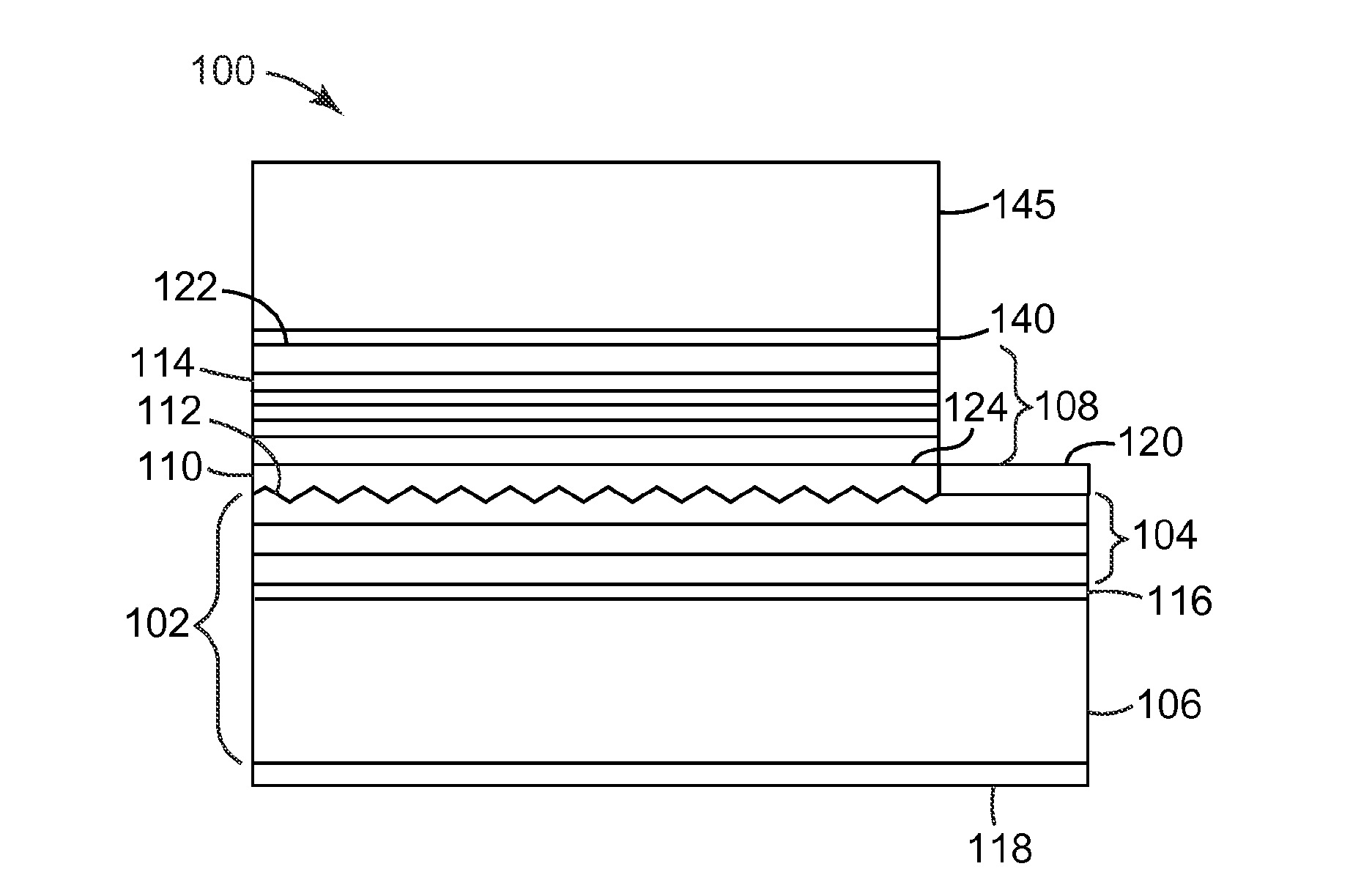
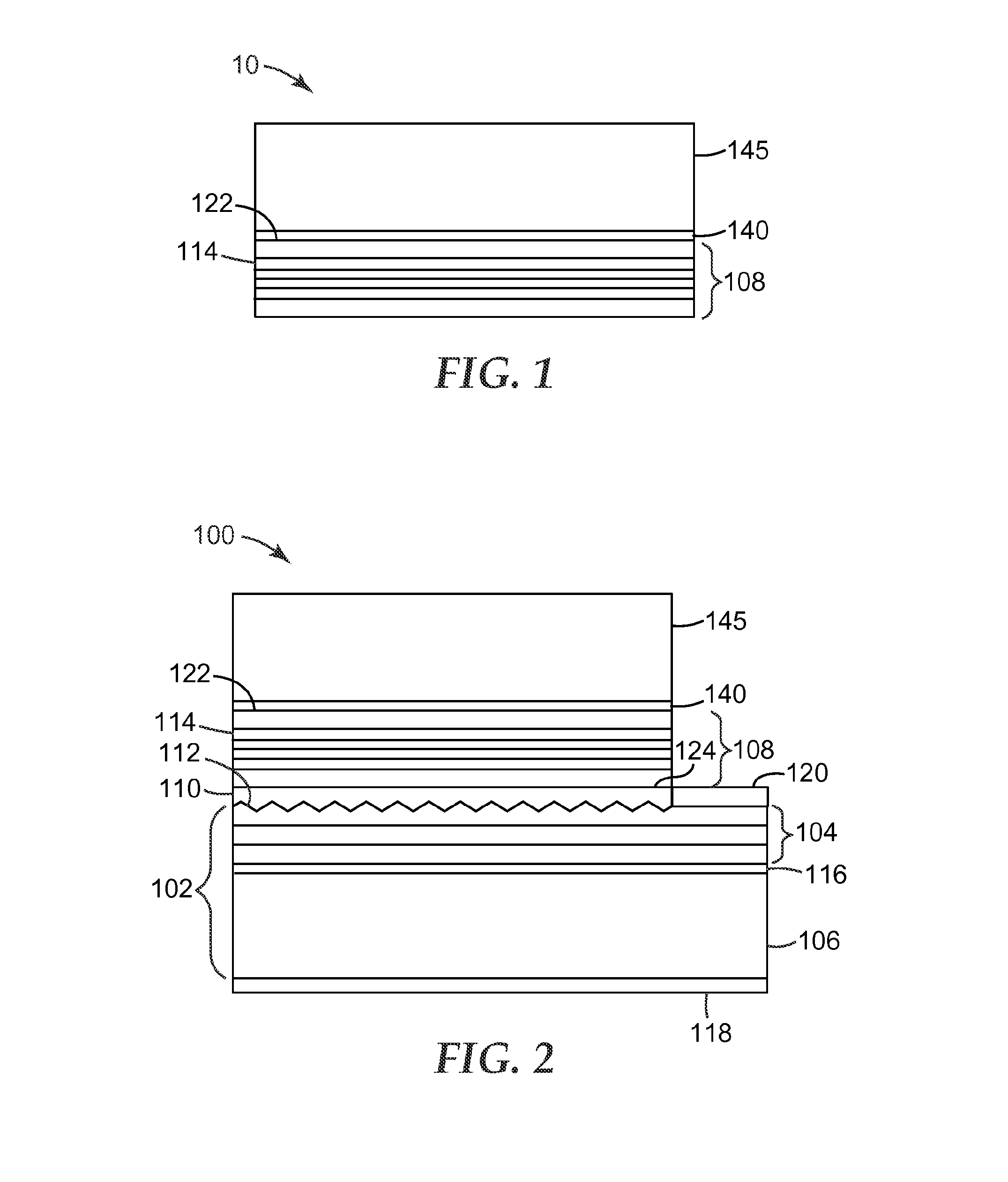
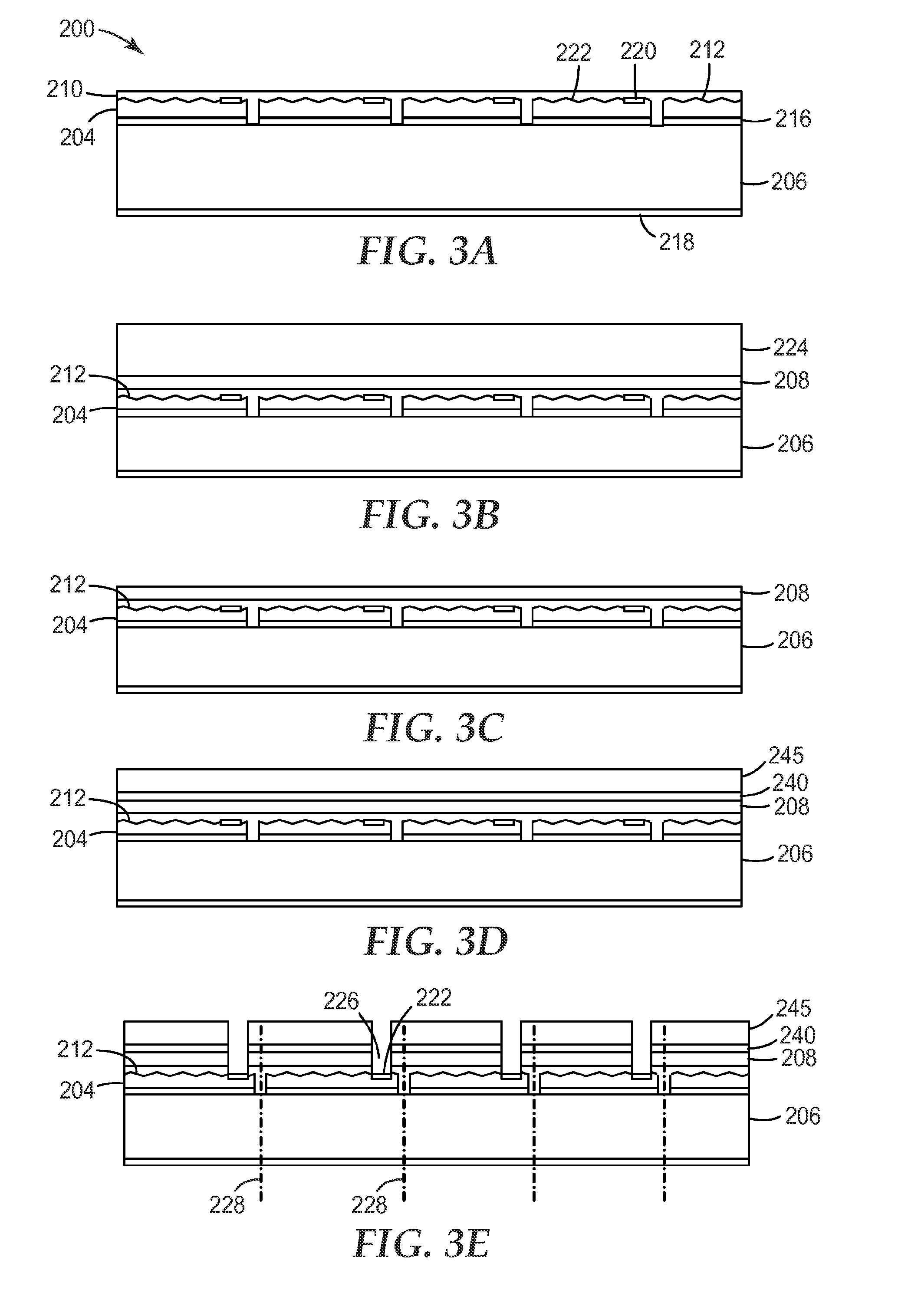
[0073]Monochrome platelets consisting of II-VI converting layers bonded to a glass wafer using polysilazane-acrylate blended adhesives were fabricated. The starting substrate consisted of a bottom substrate layer of InP with a GaInAs buffer layer followed by the II-VI converting layers on top and were grown using molecular beam epitaxial (MBE) process, similar to those described in for example in WO2009 / 048704.

[0074]To promote adhesion of the II-VI material to the final LED device, 300 nm of silicon nitride (Si3N4) and 100 nm of SiO2 were deposited onto the II-VI layer at about 100° C. using plasma enhanced chemical vapor deposition (PECVD) method. Prior to coating the Si3N4 and SiO2 layers, the surfaces of the II-VI material were reactive ion etched (RIE) with O2 plasma for 120 seconds then by argon plasma for 16 seconds.

[0075]The Si3N4 / SiO2 coated side of the II-VI material was bonded to a temporary glass carrier substrate to aid in the removal of the InP substrate and GaInAs buff...

example 2

[0084]For Example 2 a PSZ (HTT 1800)—5 weight % acrylate adhesive (SR9008) containing 1 weight % each of two initiators, dicumyl peroxide (DCP) and 2,2 dimethoxy-2 phenol acetphenone (DMAP), was prepared using the process described in Example 1.

Color Stability and % Transmission of Examples 1 and 2

[0085]For convenience, the following experiments were carried out in air except the curing process.

[0086]Approximately 10 microliters of the adhesive of Example 1 and Example 2 were each dispensed on a separate previously cleaned glass slides (2.5 cm×2.5 cm). The glass slides were cleaned in an ultrasonic bath using DI water, acetone and methanol in sequence. The slides and cover slips were then dried by blowing nitrogen gas. A previously cleaned (as described above for glass slides) glass cover slip (1 cm×1 cm) was placed on each glass slide on the adhesive drop and the cover slip were pressed lightly to spread the adhesives. Each slide-adhesive-cover slip was then radiated for 5 minutes ...

examples 3-8

[0089]Various other adhesive comprising a mixture of PSZ (HTT 1800) and various acrylate monomers were prepared using the process described in example 1. The acrylate monomer and concentration thereof is described in the following table:

Example:Acrylate used:310wt-% SR29545wt-% SR399LV55wt-% SR44465wt-% SR351LV75wt-% SR904185wt-% SR9012

[0090]The % transmission of Example 3 was evaluated in the same manner as previously described. After 4 weeks of aging at 185° C., Example 3 appeared to be thermally stable.

[0091]A study of the thermal stability of Examples 1 and 3 was conducted using thermo-gravimetric analysis (TGA). The test results indicated that such adhesives are thermally stable and usable up to about 200° C. or higher.

[0092]The % transmission of Example 3 after 5 weeks of aging at 185° C. ranged from 90% to 93% for wavelengths of 400 nm to 700 nm

[0093]The % transmission of Examples 4-8 after 5 weeks of aging at 185° C. was at least 89% for a wavelength of 400 nm and 91-93% for...


PUM


Abstract

In one embodiment, a semiconductor component, such as a wavelength converter wafer, is described wherein the wavelength converter is bonded to an adjacent inorganic component with a cured bonding layer comprising polysilazane polymer. The wavelength converter may be a multilayer semiconductor wavelength converter or an inorganic matrix comprising embedded phosphor particles. In another embodiment, the semiconductor component is a pump LED component bonded to an adjacent component with a cured bonding layer comprising polysilazane polymer. The adjacent component may the described wavelength converter(s) or another component comprised of inorganic material(s) such as a lens or a prism. Also described are methods of making semiconductor components such as wavelength converters and LED's.

Description

BACKGROUND[0001]Wavelength converted light emitting diodes (LEDs) are becoming increasingly important for illumination applications where there is a need for light of a color that is not normally generated by an LED, or where a single LED may be used in the production of light having a spectrum normally produced by a number of different LEDs together. One example of such an application is in the back-illumination of displays, such as liquid crystal display (LCD) computer monitors and televisions. In such applications there is a need for substantially white light to illuminate the LCD panel. One approach to generating white light with a single LED is to first generate blue light with the LED and then to convert some or all of the light to a different color. For example, where a blue-emitting LED is used as a source of white light, a portion of the blue light may be converted using a wavelength converter to yellow light. The resulting light, a combination of yellow and blue, appears w...

Claims


Application Information

Patent Timeline
IPC IPC(8): H01L33/50
CPCH01L33/0079H01L33/44H01L33/502H01L2933/0025H01L2924/0002H01L2933/0041H01L2924/00H01L33/0093H01L33/50
Inventor MAO, GUOPINGZNAMEROSKI, STEPHEN J.YANG, YUSMITH, TERRY L.
Owner 3M INNOVATIVE PROPERTIES CO
Why Eureka
Try Eureka