Inks and processes to make a chalcogen-containing semiconductor

Inactive Publication Date: 2013-08-29
EI DU PONT DE NEMOURS & CO
View PDF2 Cites 30 Cited by
  • Summary
  • Abstract
  • Description
  • Claims
  • Application Information

AI Technical Summary

Problems solved by technology

However, typical vacuum techniques require complicated equipment and are therefore intrinsically expensive processes.
Low-cost routes to CZTS are available, but have deficiencies.
For example, electrochemical deposition to form CZTS is an inexpensive process, but compositional non-uniformity and/or the presence of secondary phases prevents this method from generating high-quality CZTS thin-films.
This method tends to yield films of poor morphology, density and grain size.
CZTS films formed from oxyhydrate p

Method used


Image

  • Inks and processes to make a chalcogen-containing semiconductor
  • Inks and processes to make a chalcogen-containing semiconductor
  • Inks and processes to make a chalcogen-containing semiconductor

Examples


example 1

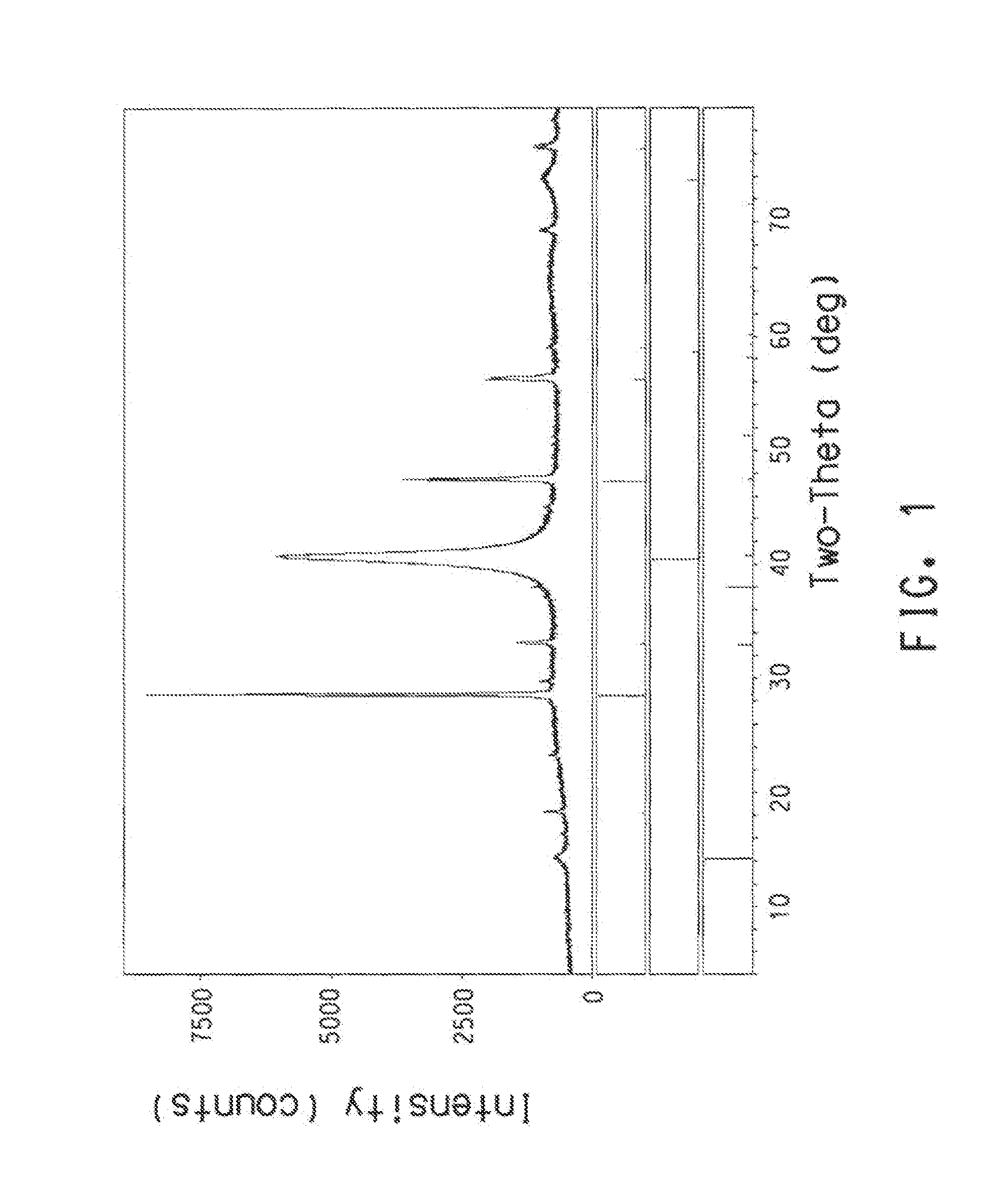
[0142]SnS and ZnS nanoparticles (prepared as described above) were individually dispersed in THF at a concentration of 500 mg nanoparticles per mL THF. Each suspension was sonicated in a bath sonicator for 30 min and then with an ultrasonic probe for 10 min. The ZnS suspension was passed through a 1.0 micron syringe filter (Whatman, 1.0 micron GF / B w / GMF). The SnS suspension was passed through a 2.7 micron syringe filter (Whatman, 2.7 micron GF / D w / GMF). Cu nanoparticles (41.9 mg; purified as described above), 0.1540 mL of the ZnS suspension and 0.3460 mL of the SnS suspension were mixed, and the resulting mixture was then sonicated in a bath sonicator for 20 min. This ink was agitated strongly immediately prior to deposition. The ink was spin-coated onto Mo-coated glass substrates by spinning at 1000 rpm for 20 sec and then spinning at 1500 rpm for 10 sec. Then the sample was annealed in a tube furnace at 550° C. for 1 h in N2 and then at 500° C. for 1 h in a sulfur / N2 atmosphere. ...

example 1a

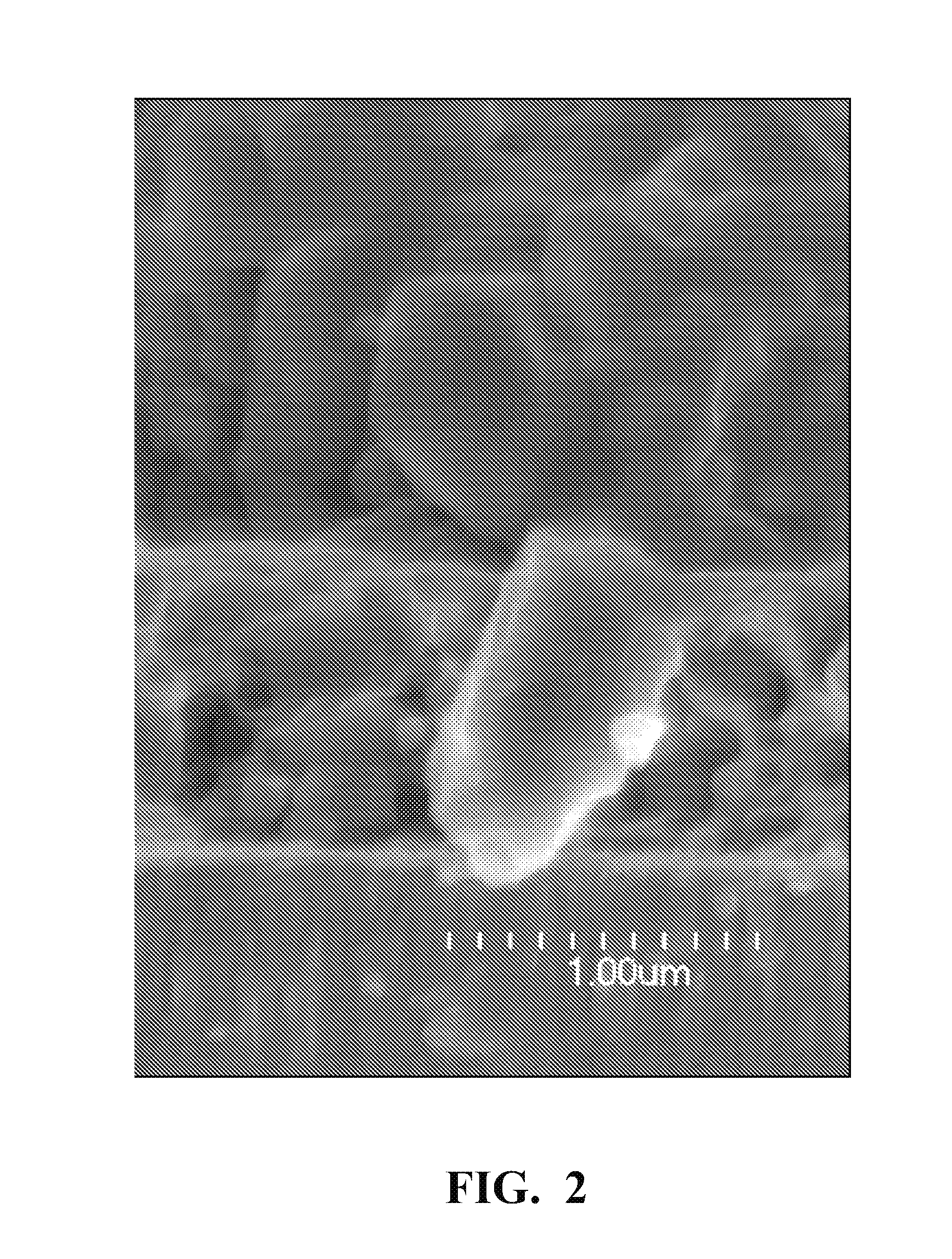
[0143]A coated substrate was prepared according to the procedure of Example 1. Profilometry of the surface was acquired in 5 different locations using a Tencor profilometer and the data was processed with a 25 micron low-pass filter, giving an average height of 1.0715 microns, an average Ra of 460 nm, and an average Wa of 231 nm for the coated substrate.

example 2

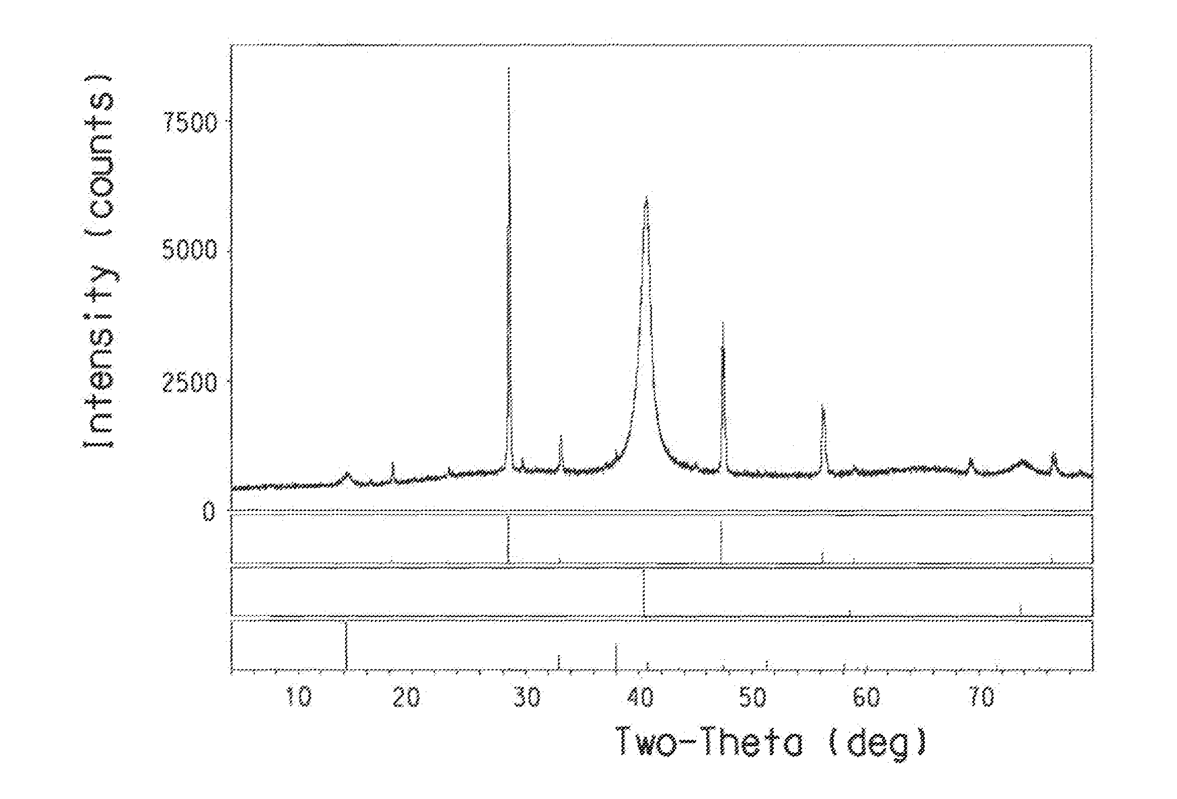
[0144]A CZTS precursor ink was prepared by dispersing commercial Sn nanosize activated powder (99.7%, 176.5 mg) from Sigma Aldrich and TEGO IL P51P (10.2 mg) in toluene (2258 mg). The dispersion was then sonicated in an ultrasonic bath for 15 min. Then CuS particles (298.9 mg) and ZnS particles (274.6 mg) were added to the Sn powder suspension. The mixture was further sonicated for 30 min in an ultrasonic bath. The CZTS precursor dispersion was spun-coated onto a molybdenum-coated glass substrate. The ink was applied to the substrate. Then the sample was spun at 200 rpm for 10 sec, followed by spinning at 350 rpm for 30 sec and a final spinning at 600 rpm for 10 sec. The coated substrate was then dried in the air at room temperature. The coated substrate was then annealed in a tube furnace at 500° C. for 2 h in a sulfur / N2 atmosphere. XRD results indicate that CZTS is the major phase in the annealed film.


PUM

PropertyMeasurementUnit
Molar ratioaaaaaaaaaa
Semiconductor propertiesaaaaaaaaaa

Abstract

The present invention relates to a process to make a chalcogen-containing semiconductor comprising copper, zinc and tin and to inks used in the process. The inks comprise at least one copper, zinc or tin source which is elemental particles of the particular metal.

Description

[0001]This application claims the benefit of U.S. Provisional Patent Application No. 61 / 416,013, filed Nov. 22, 2010 which are herein incorporated by reference.FIELD OF THE INVENTION[0002]The present invention relates to a process to make a chalcogen-containing semiconductor comprising copper, zinc and tin.BACKGROUND[0003]Thin-film photovoltaic cells typically use semiconductors such as CdTe or copper indium gallium sulfide / selenide (CIGS) as an energy absorber material. Due to the toxicity of cadmium and the limited availability of indium, alternatives are sought. Copper zinc tin sulfide (Cu2ZnSnS4 or “CZTS”) possesses a band gap energy of about 1.5 eV and a large absorption coefficient (approx. 104 cm−1), making it a promising CIGS replacement.[0004]The most common approach to fabricate CZTS thin films is to deposit elemental or binary precursors, such as Cu, Zn, Sn, ZnS, and SnS, using a vacuum technique, which is then followed by the chalcogenization of the precursors. The resul...

Claims


Application Information

Patent Timeline
IPC IPC(8): H01L21/02H01L29/26
CPCC09D11/52C23C18/1204C23C18/1229C23C18/1275H01L29/26H01L21/02568H01L21/02628H01L31/0326Y02E10/50H01L21/0237H01L31/02H01L31/0216H01L31/032
Inventor CAO, YANYANDENNY, JR., MICHAEL S.JOHNSON, LYNDA KAYELU, MEIJUNMALAJOVICH, IRINA
Owner EI DU PONT DE NEMOURS & CO
Why Eureka
Try Eureka