Substrate for CVD deposition of diamond and method for the preparation thereof
a technology of cvd deposition and substrate, which is applied in the direction of solid-state diffusion coating, transportation and packaging, coatings, etc., can solve the problems of reducing the strength of the substrate and failing to achieve the design performance of the substra
- Summary
- Abstract
- Description
- Claims
- Application Information
AI Technical Summary
Benefits of technology
Problems solved by technology
Method used
Image
Examples
example 2
[0042]86% (values indicated by mass; the same applies hereinafter) of an equal molar mixture of titanium metal fine powder (a Toho Titanium product with an average particle size of 20 μm) and amorphous boron powder was mixed with 12% of copper metal powder (each powder having a particle size of 25 μm or smaller) were further admixed with 2% of nominal 20 nm size diamond (MD20-OB grade with D50 of 23 nm, D10 of 17 nm, D90 of 38 nm; specific surface area 198 m2 / g) as surface terminated with hydrogen. The whole, as fully and intimately mixed, was kneaded with an addition of 15% of paraffin wax, extruded into a 3 mm diameter cylindrical rod, and, by firing at 700° C. in H2 to an electrode of about 75% relative density.
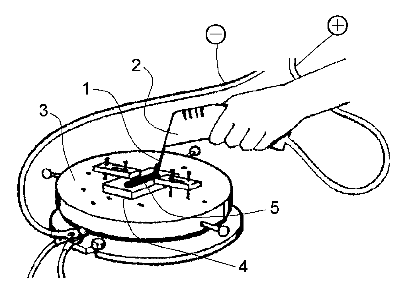
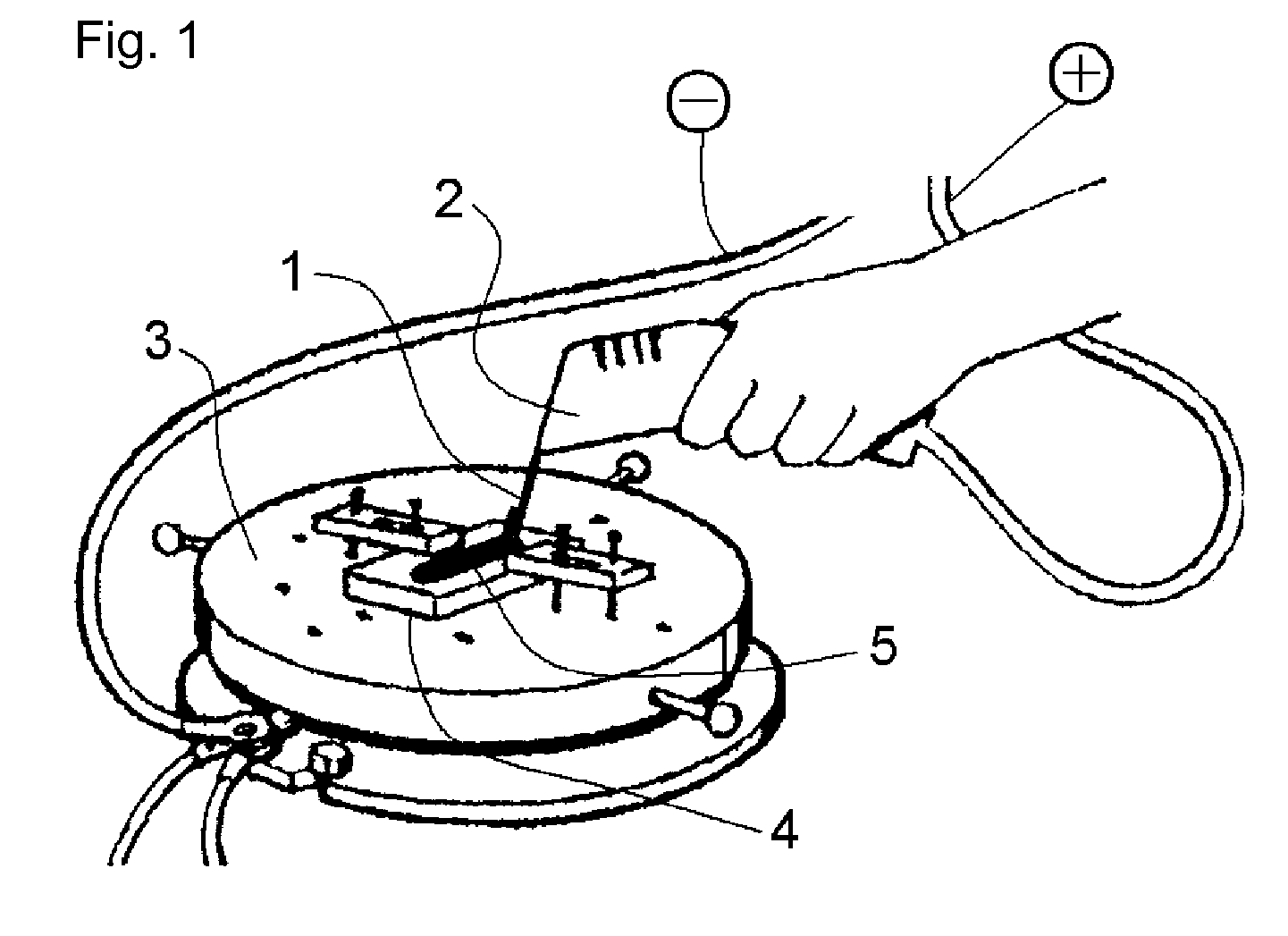
[0043]The electrode was used to operate a process likewise to Example 1 whereby a diamond containing layer was deposited at a single pulse power input E of 0.1 J, pulse frequency f of 1000 Hz and total pulse number N of 45000 on another annular plate of Co—WC.
[0044]Then a ...
example 3
[0045]Titanium metal powder (a Toho Titanium product with an average particle size of 20 μm), carbon black powder (Tokai Carbon SRF grade; average particle size of 66 nm, specific surface area of 27 m2 / g), and nominal 50 nm diamond powder (MD50-OB) were dosed to a mass proportion of 77:16:6, fully mixed intimately and press-formed to a cylindrical electrode of 5 mm in diameter and 50 mm in length with a relative density of 80%. With this electrode an electric spark discharge process was operated whereby a tungsten carbide alloy (13% Co—WC) conical tip of lathe center base was deposited on the conical surface with a 15 μm thick titanium carbide layer containing 2% approx. of diamond. The deposit was ground with a diamond wheel to provide a smooth surface, on which diamond was grown by hot filament CVD to a thickness of 15 μm.
example 4
[0046]Chromium metal powder (PKh-1, a GOST 5905-2004 product with an average particle size of 25 μm) and nominal 50 nm diamond powder (MD50-OB, Tomei Diamond product) were dosed to relative masses of 95:5. The powders were fully mixed intimately and formed to a cylindrical electrode of 5 mm in diameter and 50 mm in length with a relative density of 75%.
[0047]An electric spark discharge process was operated with an Alier-Metal power source unit whereby a lathe center conical tip base of 6% Co—WC was deposited on the surface with 25 μm thick chromium metal-chromium carbide composite layer containing 2% of diamond particles distributed in it. The deposit was lightly ground on the surface using a #400 diamond wheel to provide a smooth surface, on and over which diamond was grown by hot filament CVD to form a layer of 10 μm in thickness.
PUM
| Property | Measurement | Unit |
|---|---|---|
| particle size | aaaaa | aaaaa |
| particle size | aaaaa | aaaaa |
| size | aaaaa | aaaaa |
Abstract
Description
Claims
Application Information

