

Chemical vapor deposition of graphene on dielectrics
a dielectric and chemical vapor deposition technology, applied in chemical vapor deposition coating, plasma technique, coating, etc., can solve the problems of inability to scale up, inconvenient operation, and inability to meet the requirements of the application, and achieve low defects and high crystallinity.
- Summary
- Abstract
- Description
- Claims
- Application Information
AI Technical Summary
Benefits of technology
Problems solved by technology
Method used
Image

Examples
Embodiment Construction
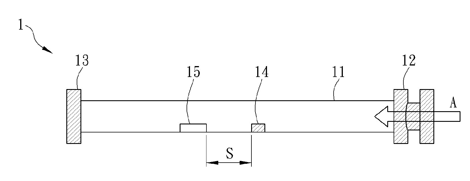
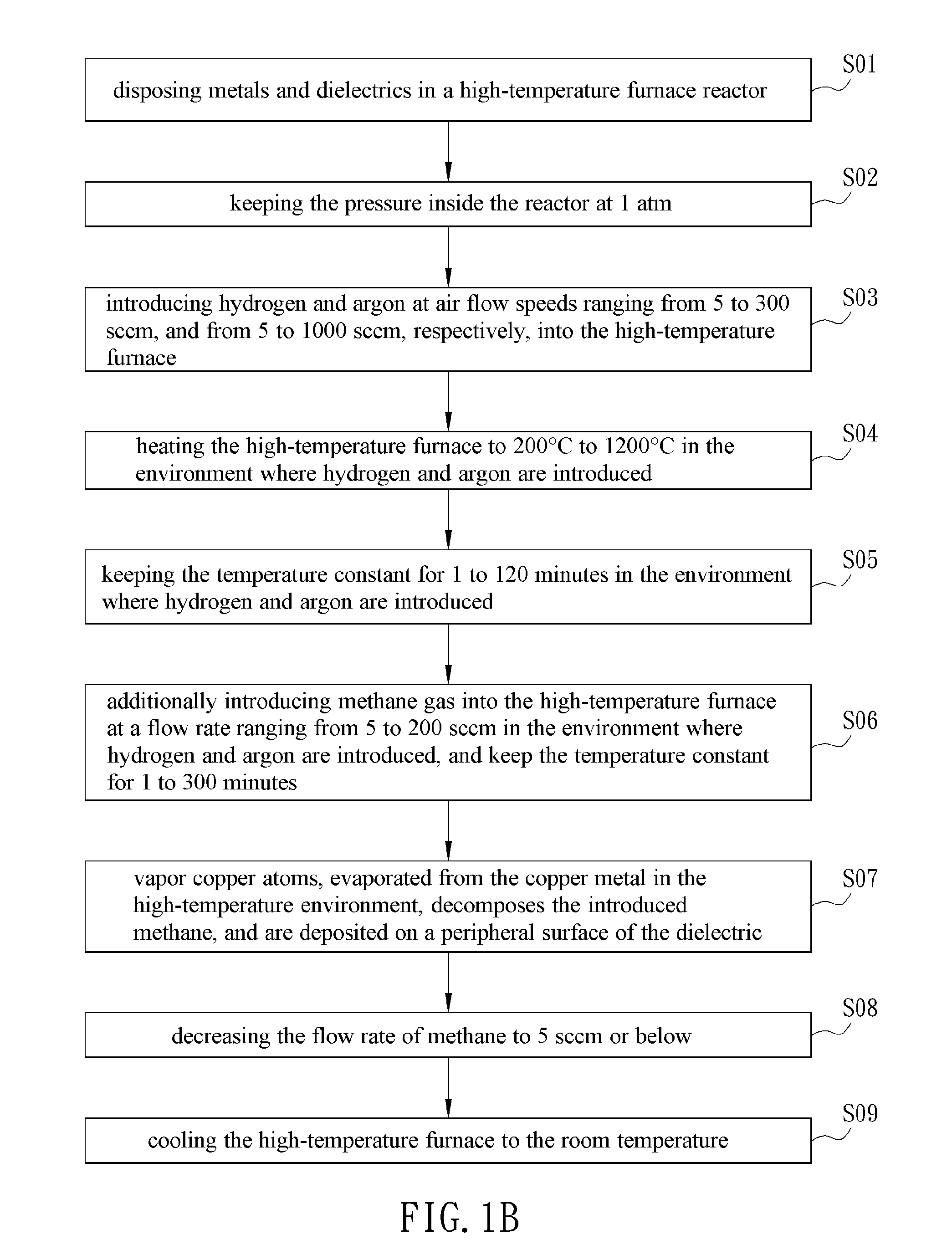
[0040]FIG. 1A is a schematic illustration showing a process apparatus 1 of growing graphene by chemical vapor deposition according to a preferred embodiment of the invention. Referring to FIG. 1A, the process apparatus 1 includes a reactor 11, an intake gate 12 and an exhaust gate 13. In this embodiment, the material of the reactor 11 is composed of quartz, ceramics or stainless steel, and the appearance of the reactor 11 is a long tubular structure with a length ranging from 50 cm to 150 cm and a diameter equal to 5 cm or 10 cm. This long tubular reactor 11 will be disposed in a heating apparatus (not shown), and the temperature inside the heating apparatus is controllable from 20° C. to 1500° C. The intake gate 12 is disposed on one end of the reactor 11, while the exhaust gate 13 is disposed on the other end of the reactor 11. The method of growing graphene by chemical vapor deposition according to a preferred embodiment of the invention includes the following steps: disposing me...
PUM
| Property | Measurement | Unit |
|---|---|---|
| Temperature | aaaaa | aaaaa |
| Temperature | aaaaa | aaaaa |
| Length | aaaaa | aaaaa |
Abstract
Description
Claims
Application Information