

Novel diblock copolymer, preparation method thereof, and method of forming NANO pattern using the same
a technology of diblocks and copolymers, which is applied in the field of new diblock copolymers, can solve the problems of limiting the use of photolithography, unable to simultaneously form two-dimensional patterns, and difficult to fabricate printed circuits of 30 nm or less, etc., to facilitate the formation of nanostructures, easy to form, and easy to patterned
- Summary
- Abstract
- Description
- Claims
- Application Information
AI Technical Summary
Benefits of technology
Problems solved by technology
Method used
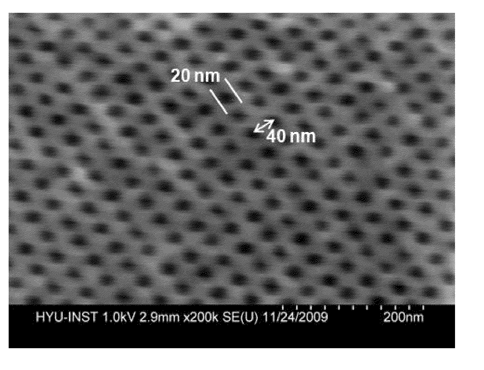
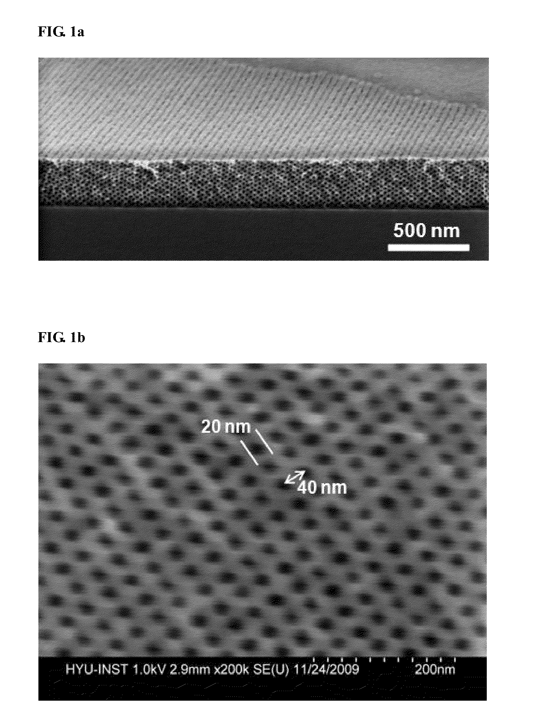
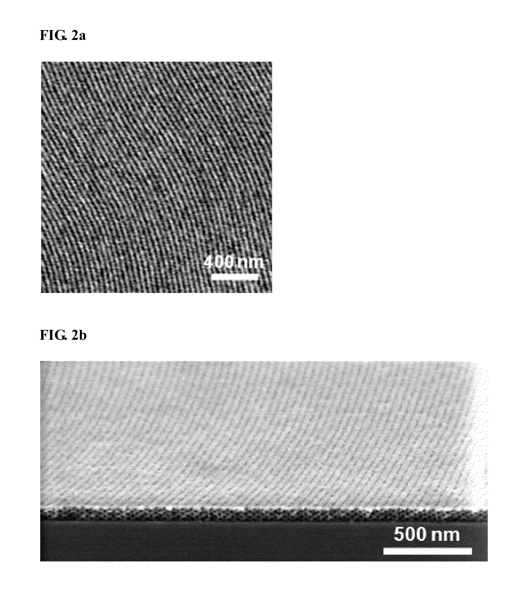
Image

Examples
examples 1 and 2
Synthesis of Acrylamide-Based Monomer and Identification of Crystallinity
example 1
Synthesis of p-Dodecylphenylacrylamide (DOPAM) and Preparation of Single Crystal
[0096]Firstly, p-dodecylaniline (12 g, 0.046 mol) was dissolved in a THF solvent (100 mL). The solution was poured into a 100 mL three-necked round flask, and an acid scavenger containing imidazole and triethyl amine at the same mole fraction (0.023 mol) was added dropwise through a funnel for 10 minutes. Under nitrogen atmosphere, a solution containing acryloyl chloride (3.8 mL, 0.047 mol) in THF (20 mL) was gradually added dropwise to the mixed solution through a dropping funnel for 20 minutes. Meanwhile, the solution was cooled on an ice bath to prevent the temperature of the reaction mixture from rising above 5° C. After 6 hours of reaction at 0° C., the solution was kept at 25° C. for more 9 hours of reaction. Upon completion of the reaction, the solution was passed through a filter paper to eliminate precipitated salts, and the solvent was evaporated from the filtrate on an evaporator. The solid th...
example 2
Synthesis of p-Tetradecylphenylacrylamide (TEPAM) and p-hexadecylphenylacrylamide (HEPAM) and Preparation of Single Crystal
[0100]TEPAM and HEPAM were synthesized with the yields of 90% and 93%, respectively in the same manner as described in Example 1, except that p-tetradecylaniline having 14 carbon atoms or p-hexadecylaniline having 16 carbon atoms was used instead of p-dodecylaniline having 12 carbon atoms. The single crystals of TEPAM and HEPAM were grown and identified by XRD analysis in the same manner as described in Example 1, confirming that the single crystals had a monoclinic crystal structure.
PUM
| Property | Measurement | Unit |
|---|---|---|
| mol % | aaaaa | aaaaa |
| mol % | aaaaa | aaaaa |
| mol % | aaaaa | aaaaa |
Abstract
Description
Claims
Application Information