Replacement gate with reduced gate leakage current

a technology of leakage current and replacement gate, which is applied in the direction of semiconductor devices, transistors, electrical apparatus, etc., can solve the problems of limiting the performance of conventional semiconductor oxide based gate electrodes, and the challenge has been particularly difficult, and achieves the effect of improving the performance of an n-type field effect transistor

Inactive Publication Date: 2013-10-03
GLOBALFOUNDRIES INC
View PDF6 Cites 50 Cited by
  • Summary
  • Abstract
  • Description
  • Claims
  • Application Information

AI Technical Summary

Benefits of technology

[0006]Replacement gate work function material stacks are provided, which provide a work function about the energy level of the conduction band of silicon. After removal of a disposable gate stack, a gate dielectric layer is formed in a gate cavity. A metallic compound layer including a metal and a non-metal element is deposited directly on the gate dielectric layer. At least one barrier layer and a conductive material layer are deposited and planarized to fill the gate cavity. The metallic compound layer includes a material, which provides, in combination with other layers, a work function about 4.0 eV, and specifically, less than 4.4 eV, and can include a material selected from tantalum carbide, metallic nitrides, and a hafnium-silicon alloy. Thus, the metallic compound layer can provide a work function that enhances the performance of an n-type field effect transistor employing a silicon channel.

Problems solved by technology

High gate leakage current of silicon oxide and nitrided silicon dioxide as well as depletion effect of polysilicon gate electrodes limits the performance of conventional semiconductor oxide based gate electrodes.
A challenge in semiconductor technology has been to provide two types of gate electrodes having a first work function at or near the valence band edge and a second work function at or near the conduction band edge of the underlying semiconductor material such as silicon.
This challenge has been particularly difficult because the two types of gate electrodes are also required to be a metallic material having a high electrical conductivity.

Method used


Image

  • Replacement gate with reduced gate leakage current
  • Replacement gate with reduced gate leakage current
  • Replacement gate with reduced gate leakage current

Examples


first embodiment

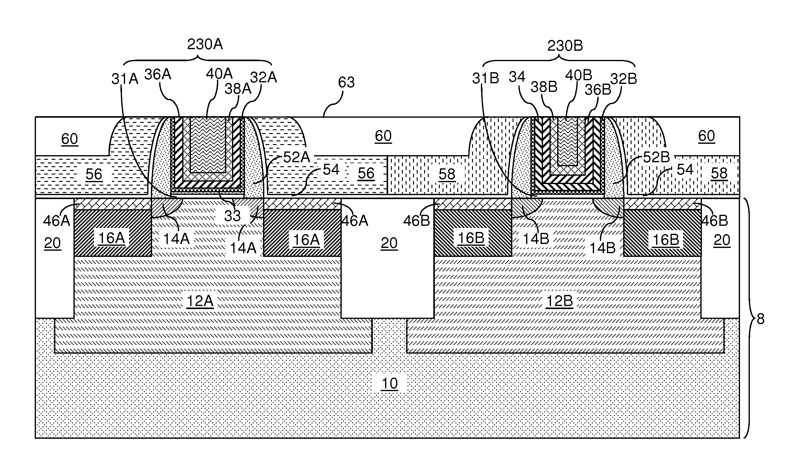
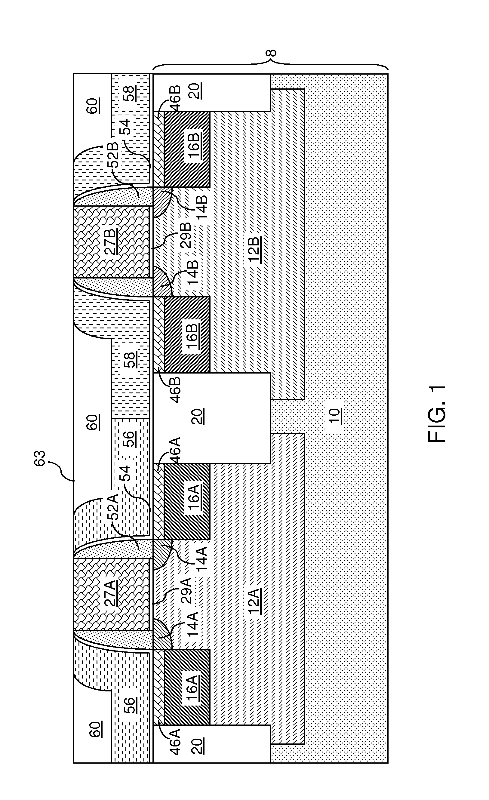
[0041]Referring to FIG. 1, a first exemplary semiconductor structure according to the present disclosure includes a semiconductor substrate 8, on which various components of field effect transistors are formed. The semiconductor substrate 8 can be a bulk substrate including a bulk semiconductor material throughout, or a semiconductor-on-insulator (SOI) substrate (not shown) containing a top semiconductor layer, a buried insulator layer located under the top semiconductor layer, and a bottom semiconductor layer located under the buried insulator layer.

[0042]Various portions of the semiconductor material in the semiconductor substrate 8 can be doped with electrical dopants of n-type or p-type at different dopant concentration levels. For example, the semiconductor substrate 8 may include an underlying semiconductor layer 10, a first doped well 12A formed in a first device region (the region to the left in FIG. 1), and an second doped well 12B formed in a second device region (the regi...

second embodiment

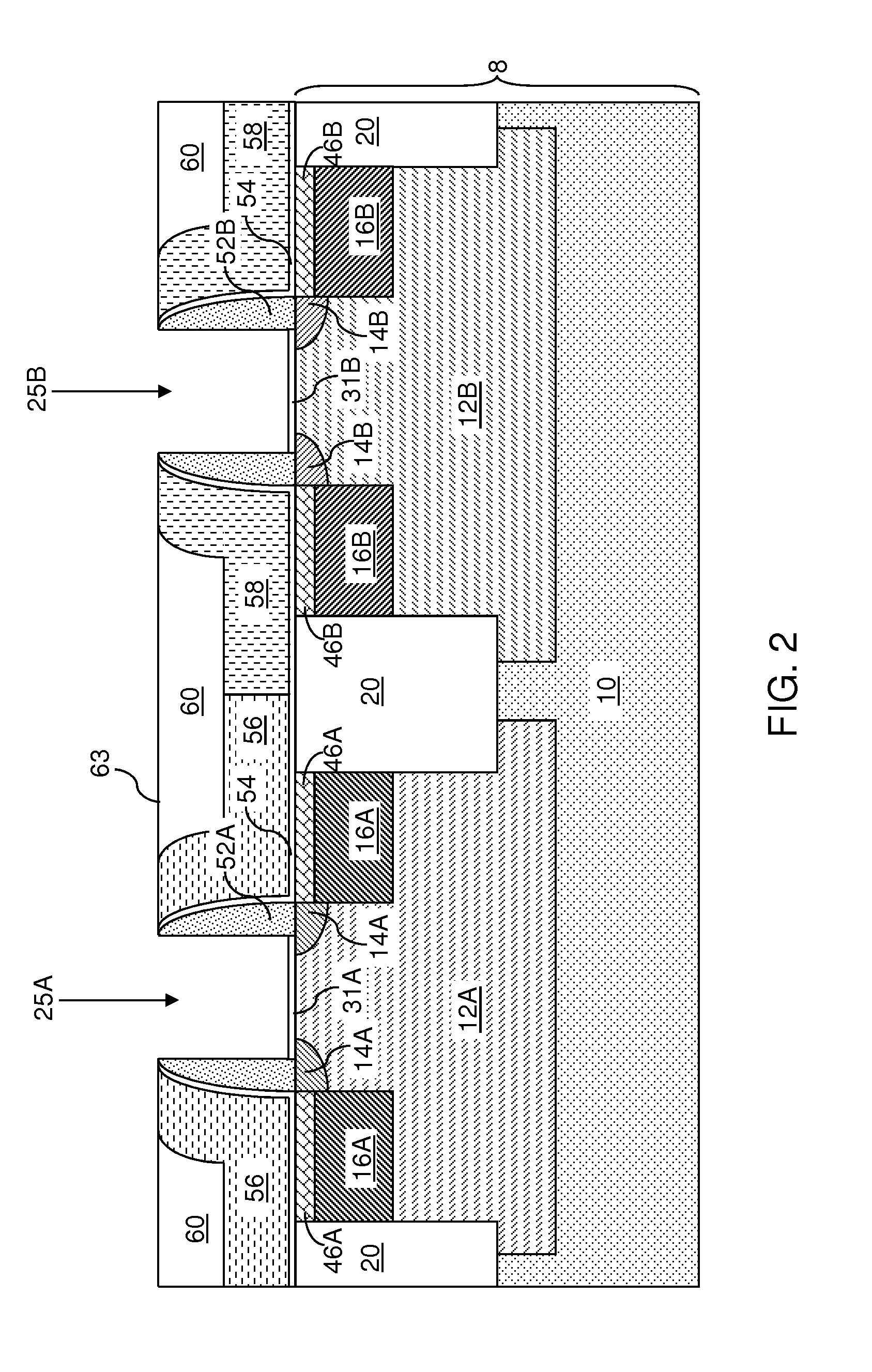
[0098]Referring to FIG. 19, a second exemplary semiconductor structure according to the present disclosure is derived from the first exemplary semiconductor structure of FIG. 1A by removing the first and second disposable gate material portions (27A, 27B) selective to the dielectric materials of the planarization dielectric layer 60, the first stress-generating liner 58 and / or the second stress-generating liner 56 (if present), and the first and second dielectric gate spacers (52A, 52B). The disposable dielectric portions (29A, 29B) may, or may not, be removed at this step.

[0099]An optional dielectric liner 230L may be applied over the planarization dielectric layer 60 and within the first and second gate cavities (25A, 25B; See FIG. 2). A photoresist layer 239 is applied over the optional dielectric liner 230L or over the planarization dielectric layer 60 and within the first and second gate cavities (25A, 25B). The photoresist layer 239 is lithographically patterned by lithographi...

third embodiment

[0103]Referring to FIG. 23, a third exemplary semiconductor structure according to the present disclosure is derived from the first exemplary semiconductor structure of FIG. 1A by removing the first and second disposable gate material portions (27A, 27B) selective to the dielectric materials of the planarization dielectric layer 60, the first stress-generating liner 58 and / or the second stress-generating liner 56 (if present), and the first and second dielectric gate spacers (52A, 52B). The disposable dielectric portions (29A, 29B) may, or may not, be removed at this step.

[0104]An optional dielectric liner 230L may be applied over the planarization dielectric layer 60 and within the first and second gate cavities (25A, 25B; See FIG. 2). A photoresist layer 239 is applied over the optional dielectric liner 230L or over the planarization dielectric layer 60 and within the first and second gate cavities (25A, 25B). The photoresist layer 239 is lithographically patterned by lithographic...


PUM


Abstract

Replacement gate work function material stacks are provided, which provides a work function about the energy level of the conduction band of silicon. After removal of a disposable gate stack, a gate dielectric layer is formed in a gate cavity. A metallic compound layer including a metal and a non-metal element is deposited directly on the gate dielectric layer. At least one barrier layer and a conductive material layer is deposited and planarized to fill the gate cavity. The metallic compound layer includes a material, which provides, in combination with other layer, a work function about 4.4 eV or less, and can include a material selected from tantalum carbide, metallic nitrides, and a hafnium-silicon alloy. Thus, the metallic compound layer can provide a work function that enhances the performance of an n-type field effect transistor employing a silicon channel. Optionally, carbon doping can be introduced in the channel.

Description

CROSS REFERENCE TO RELATED APPLICATION[0001]This application is a continuation of U.S. patent application Ser. No. 13 / 430,755, filed Mar. 27, 2012 the entire content and disclosure of which is incorporated herein by reference.BACKGROUND[0002]The present disclosure generally relates to semiconductor devices, and particularly to semiconductor structures having dual work function material gates and a high-k gate dielectric, and methods of manufacturing the same.[0003]High gate leakage current of silicon oxide and nitrided silicon dioxide as well as depletion effect of polysilicon gate electrodes limits the performance of conventional semiconductor oxide based gate electrodes. High performance devices for an equivalent oxide thickness (EOT) less than 2 nm require high dielectric constant (high-k) gate dielectrics and metal gate electrodes to limit the gate leakage current and provide high on-currents. Materials for high-k gate dielectrics include ZrO2, HfO2, other dielectric metal oxide...

Claims


Application Information

Patent Timeline
Patent Type & Authority Applications(United States)
IPC IPC(8): H01L21/285
CPCH01L21/28518H01L21/823842H01L21/26506H01L21/823857H01L21/28088H01L21/28176H01L29/4966H01L29/517H01L29/518H01L29/66545H01L29/6659H01L29/7833H01L29/7848H01L29/105H01L21/823807
Inventor JAGANNATHAN, HEMANTHDIVAKARUNI, RAMACHANDRAKWON, UNOHNARAYANAN, VIJAYRAMACHANDRAN, RAVIKUMAR
Owner GLOBALFOUNDRIES INC
Why Eureka
Try Eureka