

Organic field-effect transistor device
Patent Information
- Authority / Receiving Office
- US · United States
- Current Assignee / Owner
- ACREO SWEDISH ICT
- Publication Date
- 2013-10-17
- Estimated Expiration
- Not applicable · inactive patent
Smart Images
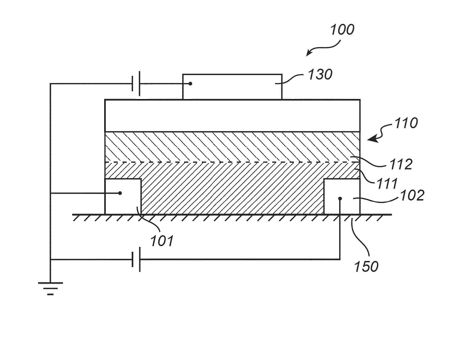
Figure 1 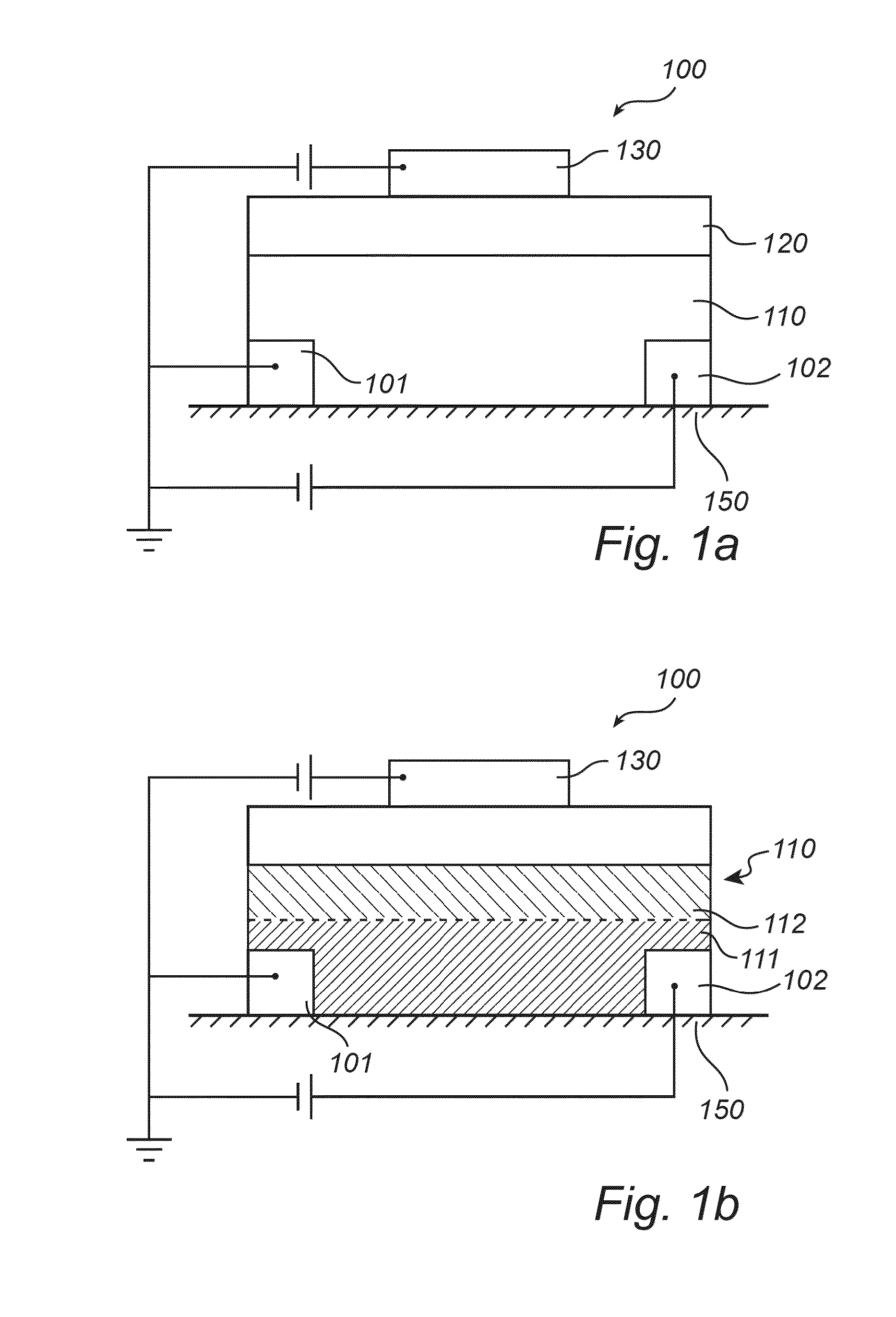
Figure 2 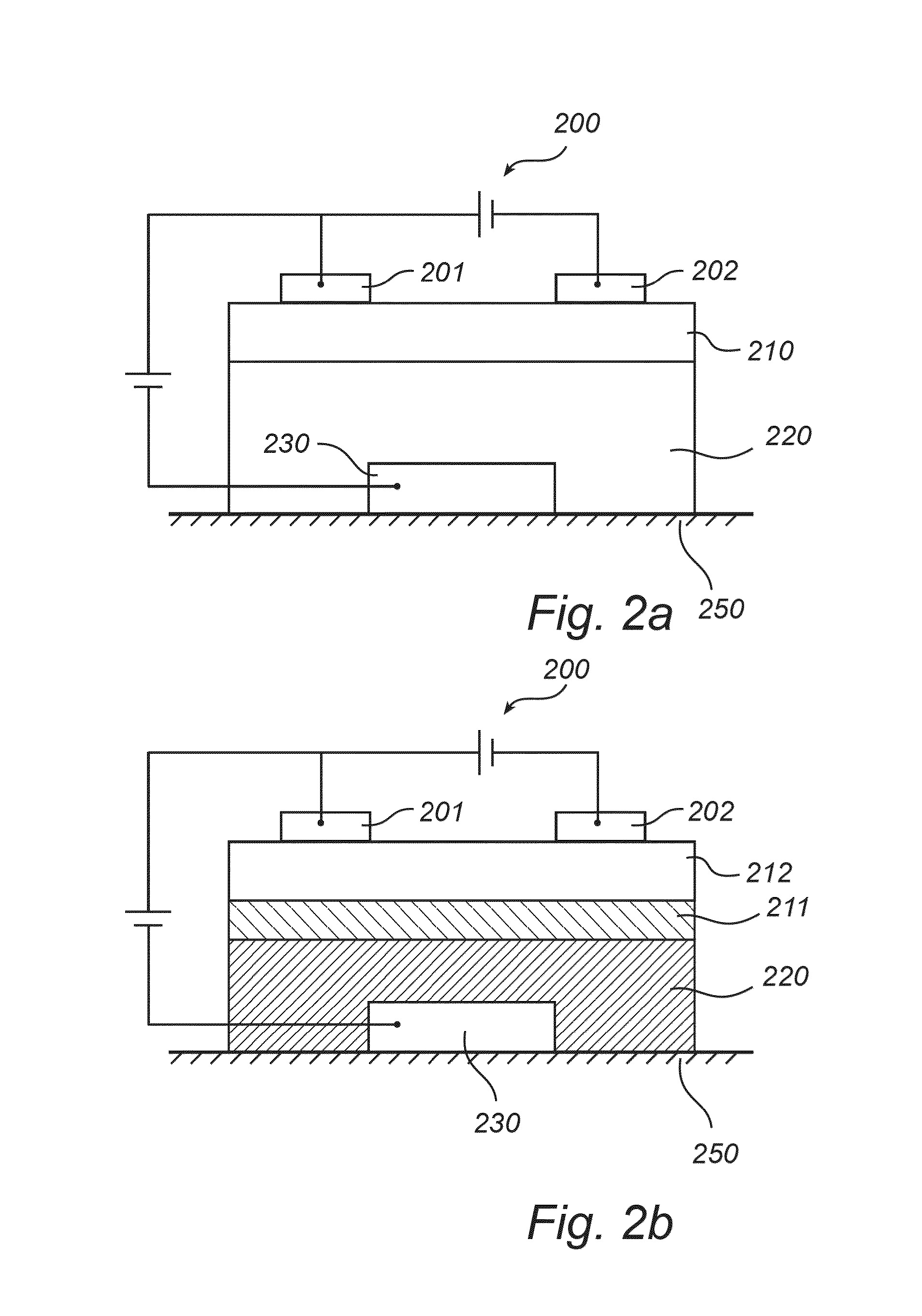
Figure 3
Abstract
Description
CROSS-REFERENCE TO RELATED APPLICATIONS
[0001] This application claims priority under 35 U.S.C. §119(a) from U.S. Provisional Patent Application No. 61 / 623,632 filed on Apr. 13, 2012, and European Application No. 12164095.7 filed on Apr. 13, 2012, the disclosures of each of which are hereby incorporated by reference in their entirety.THE TECHNICAL FIELD
[0002] The invention relates to organic field-effect transistor device comprising a semiconductor layer of semiconducting polymeric material, to a method for producing the device, to semiconducting polymeric materials and a method for producing the material.BACKGROUND ART
[0003] There are organic field effect transistors (OFET) comprising polymeric semiconducting polymers known
[0004] Transistors comprising polyelectrolytes are previous known but problems with electrochemical effects may appear. Also, solutions to avoid the bulk electrochemistry have been presented and they have shown to be fast.
[0005] However, when the transistors are produc...