Laminated structure, member for semiconductor manufacturing apparatus, and method for producing laminated structure

a technology of semiconductor manufacturing apparatus and laminated structure, which is applied in the direction of electrical equipment, magnetic recording, recording information storage, etc., can solve the problems of laminated product defects, and achieve the effects of reducing the formation of reaction layers, reducing defects, and increasing stress

Active Publication Date: 2014-03-20
NGK INSULATORS LTD
View PDF4 Cites 14 Cited by
  • Summary
  • Abstract
  • Description
  • Claims
  • Application Information

AI Technical Summary

Benefits of technology

[0009]In view of the situation described above, it is a principal object of the present invention to provide a laminated structure in which a plurality of structures each having a given thickness are stacked and can reduce the occurrence of defects, member for a semiconductor manufacturing apparatus, and a method for producing the laminated structure.
[0010]As a result of extensive studies to achieve the principal object, the present inventors completed the present invention by finding that sintering a second structure containing grain boundary phases of a rare-earth aluminum composite oxide having a garnet-type crystal structure (RE3Al5O12, wherein RE denotes a rare-earth metal element) formed on a first structure containing a main phase of magnesium-aluminum oxynitride while minimizing the difference in linear thermal expansion coefficient between the first structure and the second structure can suppress the formation of a reaction layer containing a smaller amount of grain boundary phases between the first structure and the second structure, thereby reducing the occurrence of defects.
[0014]A laminated structure, a member for a semiconductor manufacturing apparatus, and a method for producing the laminated structure according to the present invention can reduce the occurrence of defects in the laminated structure in which a plurality of structures each having a given thickness are stacked. The reason for this is not clear but may be assumed as described below. For example, when the difference in linear thermal expansion coefficient between the first structure and the second structure is 0.3 ppm / K or less, because of the small difference in linear thermal expansion coefficient between the first structure and the second structure, bonding of the structures at high temperatures for example, bonding by sintering) or repeated use of the laminated structure at high temperature and low temperature rarely causes cracking or detachment. For example, when the first structure containing magnesium-aluminum oxynitride and the second structure containing grain boundary phases of a monoclinic-type rare-earth aluminum composite oxide (RE4Al2O9, wherein RE denotes a rare-earth metal element) are laminated and fired, it is supposed that the grain boundary phases of the second structure can easily diffuse into the first structure to form a thicker reaction layer containing a smaller amount of grain boundary phases of the rare-earth aluminum composite oxide. A larger difference in thickness between the first structure and the second structure results in greater stress during the sintering process and a greater number of defects, such as cracks. In contrast, use of the second structure containing grain boundary phases of the garnet-type rare-earth aluminum composite oxide can reduce the diffusion of the grain boundary phases of the second structure into the first structure and thereby reduce the formation of the reaction layer. This can probably reduce the number of defects, such as cracks, in the laminated structure.

Problems solved by technology

In the laminated product described in Patent Literature 2, however, when the corrosion-resistant layer and the substrate layer have very different thicknesses, the laminated product may have defects, such as a crack.

Method used


Image

  • Laminated structure, member for semiconductor manufacturing apparatus, and method for producing laminated structure
  • Laminated structure, member for semiconductor manufacturing apparatus, and method for producing laminated structure
  • Laminated structure, member for semiconductor manufacturing apparatus, and method for producing laminated structure

Examples


examples

[0052]Specific examples of the production of a laminated structure will be described in the following examples.

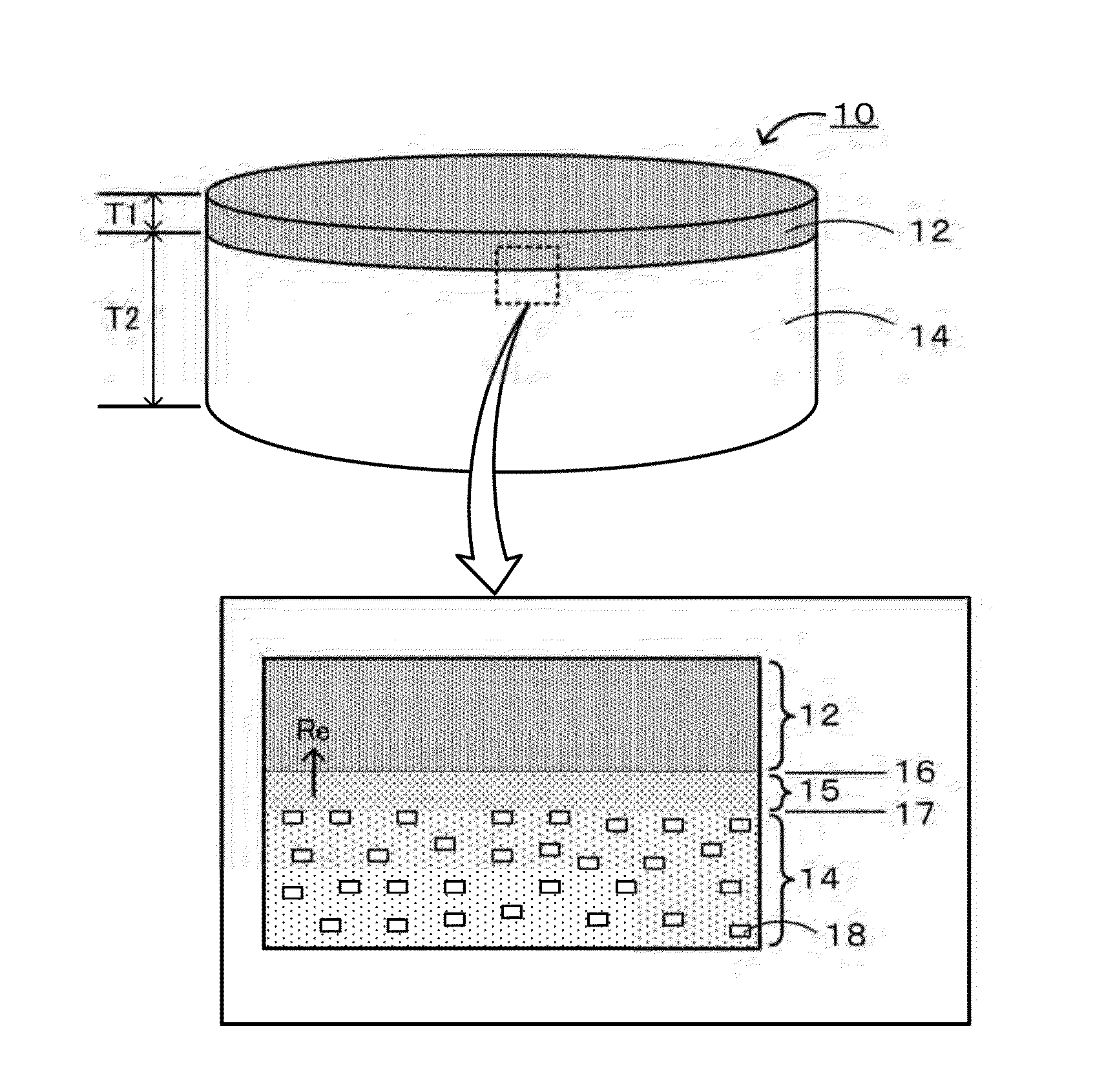
[0053](Forming Process of First Structure)

[0054]An AlN raw material, a MgO raw material, and an Al2O3 raw material were weighed so as to satisfy the mol % values listed in Table 1 and were wet-blended in an isopropyl alcohol solvent in a nylon pot using iron-core nylon balls having a diameter of 20 mm for four hours. The AlN raw material, the MgO raw material, and the Al2O3 raw material were commercial products each having a purity of 99.9% by mass or more and an average particle size of 1 μm or less. Since the AlN raw material inevitably contains 1% by mass oxygen, oxygen was not counted as an impurity element to determine the purity. After blending, the resulting slurry was removed and was dried in a nitrogen stream at 110° C. The dried product was passed through a 30-mesh sieve to prepare a mixed powder of the first structure. The mixed powder was subjected to uniaxial p...

examples 1 to 3

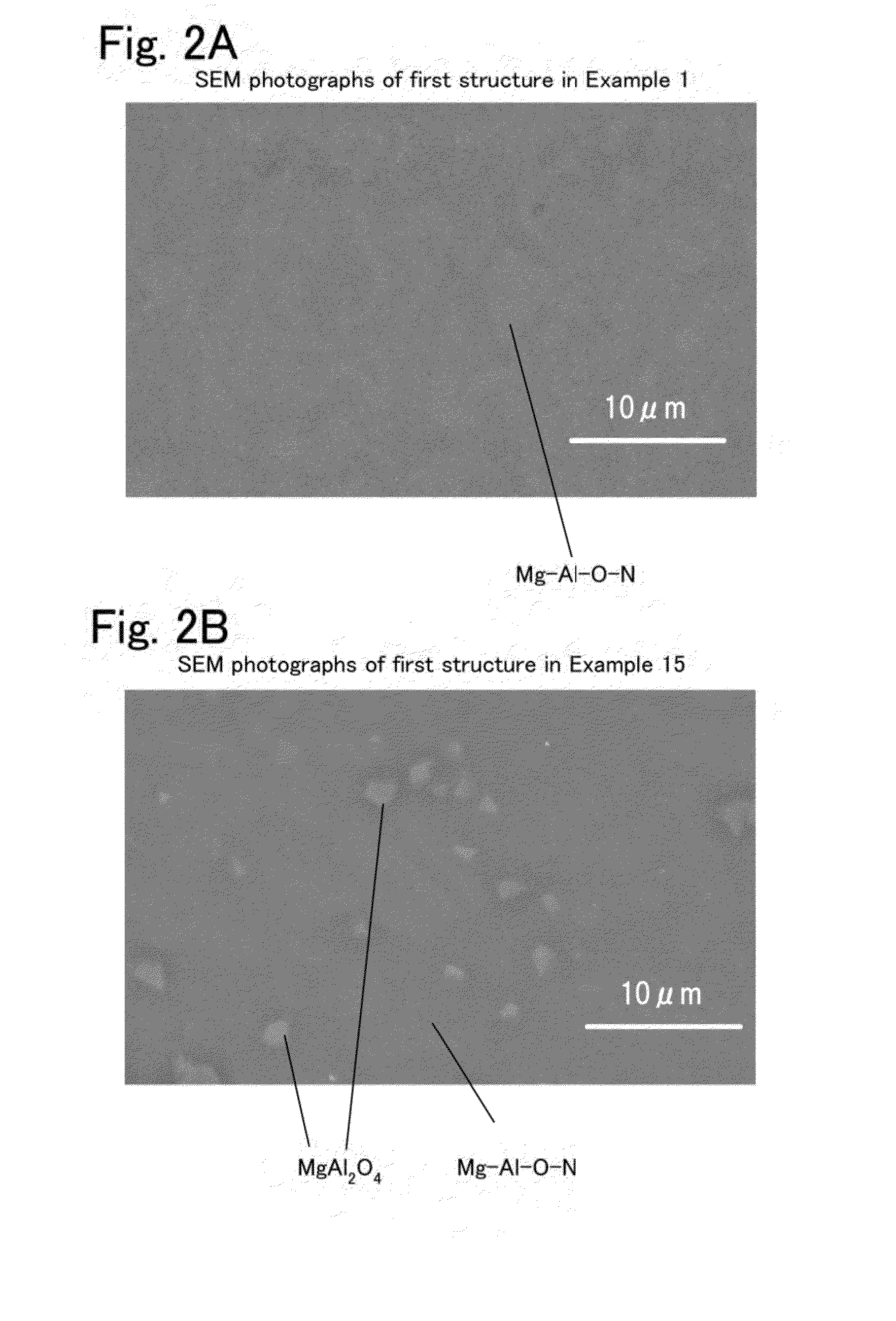
[0058]The first structure was formed by mixing 80.3 mol % AlN raw material, 10.9 mol % MgO raw material, and 8.8 mol % Al2O3 raw material and sintering at a temperature of 1950° C. The second structure was formed by mixing 93.5 mol % AlN raw material, 2.7 mol % Y2O3 raw material, and 3.8 mol % Al2O raw material and sintering at a temperature of 1700° C. The resulting laminated structure was referred to as Example 1. Laminated structures according to Examples 2 and 3 were formed in the same manner as in Example 1 except that the sintering temperatures of the laminated products were 1750° C. and 1800° C., respectively.

examples 4 to 8

[0060]A laminated structure according to Example 4 was formed in the same manner as in Example 1 except that 98.8 mol %. AlN raw material, 0.7 mol % Y2O3 raw material, and 0.5 mol % Al2O3 raw material were mixed and fired at a sintering temperature of 1800° C. to form the second structure. A laminated structure according to Example 5 was formed in the same manner as in Example 4 except that 96.9 mol % Al2O3 raw material, 1.7 mol % Y2O3 raw material, and 1.4 mol % Al2O3 raw material were mixed to form the second structure. A laminated structure according to Example 6 was formed in the same manner as in Example 4 except that 97,0 mol % AlN raw material, 1.5 mol % Y2O3 raw material, and 1.5 mol % Al2O3 raw material were mixed to form the second structure. A laminated structure according to Example 7 was formed in the same manner as in Example 4 except that 95.4 mol % AlN raw material, 2.0 mol % Y2O3 raw material, and 2.6 mol % Al2O3 raw material were mixed to form the second structure....


PUM

PropertyMeasurementUnit
thicknessaaaaaaaaaa
thicknessaaaaaaaaaa
aaaaaaaaaa

Abstract

A laminated structure 10 includes a first structure 12 containing a main phase of magnesium-aluminum oxynitride, a second structure 14 containing a main phase of aluminum nitride and grain boundary phases of a rare-earth aluminum composite oxide having a garnet-type crystal structure, and a reaction layer 15 formed between the first structure 12 and the second structure 14. The reaction layer 15 is an aluminum nitride layer containing a smaller amount of grain boundary phases 18 of the rare-earth aluminum composite oxide than the second structure 14. The reaction layer 15 of the laminated structure 10 has a thickness of 150 μm or less. The reaction layer 15 is formed during the sintering by diffusing the grain boundary phases 18 into the first structure 12.

Description

BACKGROUND OF THE INVENTION[0001]1. Field of the Invention[0002]The present invention relates to a laminated structure, a member for a semiconductor manufacturing apparatus, and a method for producing the laminated structure.[0003]2. Description of the Related Art[0004]Reactive plasma of a halogen, such as F of Cl, for etching or cleaning is used in a semiconductor manufacturing apparatus for use in a dry process or plasma coating in semiconductor manufacturing. Thus, members for use in such a semiconductor manufacturing apparatus require high corrosion resistance and generally include members composed of corrosion-resistant metals, such as aluminum subjected to alumite treatment and Hastelloy, and ceramics. In particular, electrostatic chuck members and heater members for supporting and fixing a Si wafer require high corrosion resistance and low dusting and are therefore made of corrosion-resistant ceramics, such as aluminum nitride, alumina, and sapphire. Even such ceramic materia...

Claims


Application Information

Patent Timeline
Patent Type & Authority Applications(United States)
IPC IPC(8): H01L21/683B32B18/00
CPCB32B18/00H01L21/6833C04B35/58C04B35/581C04B35/645C04B2235/3206C04B2235/3217C04B2235/3222C04B2235/3224C04B2235/3225C04B2235/3865C04B2235/3869C04B2235/72C04B2235/80C04B2235/9607C04B2237/366C04B2237/60H01J37/3222H01J37/32238H01J37/32477H01J37/3255H01J37/32715Y10T428/265H01L21/02H01L21/683
Inventor JINDO, ASUMIINOUE, KATSUHIROKATSUDA, YUJI
Owner NGK INSULATORS LTD
Why Eureka
Try Eureka