Method for manufacturing ion optical device
- Summary
- Abstract
- Description
- Claims
- Application Information
AI Technical Summary
Benefits of technology
Problems solved by technology
Method used
Image
Examples
first embodiment
[0034]1. Prepare a Substrate
[0035]In this embodiment, ceramic is selected as a substrate material for machining. The ceramic may be, for example, alumina, zirconia, or a mixture thereof according to a proportion.
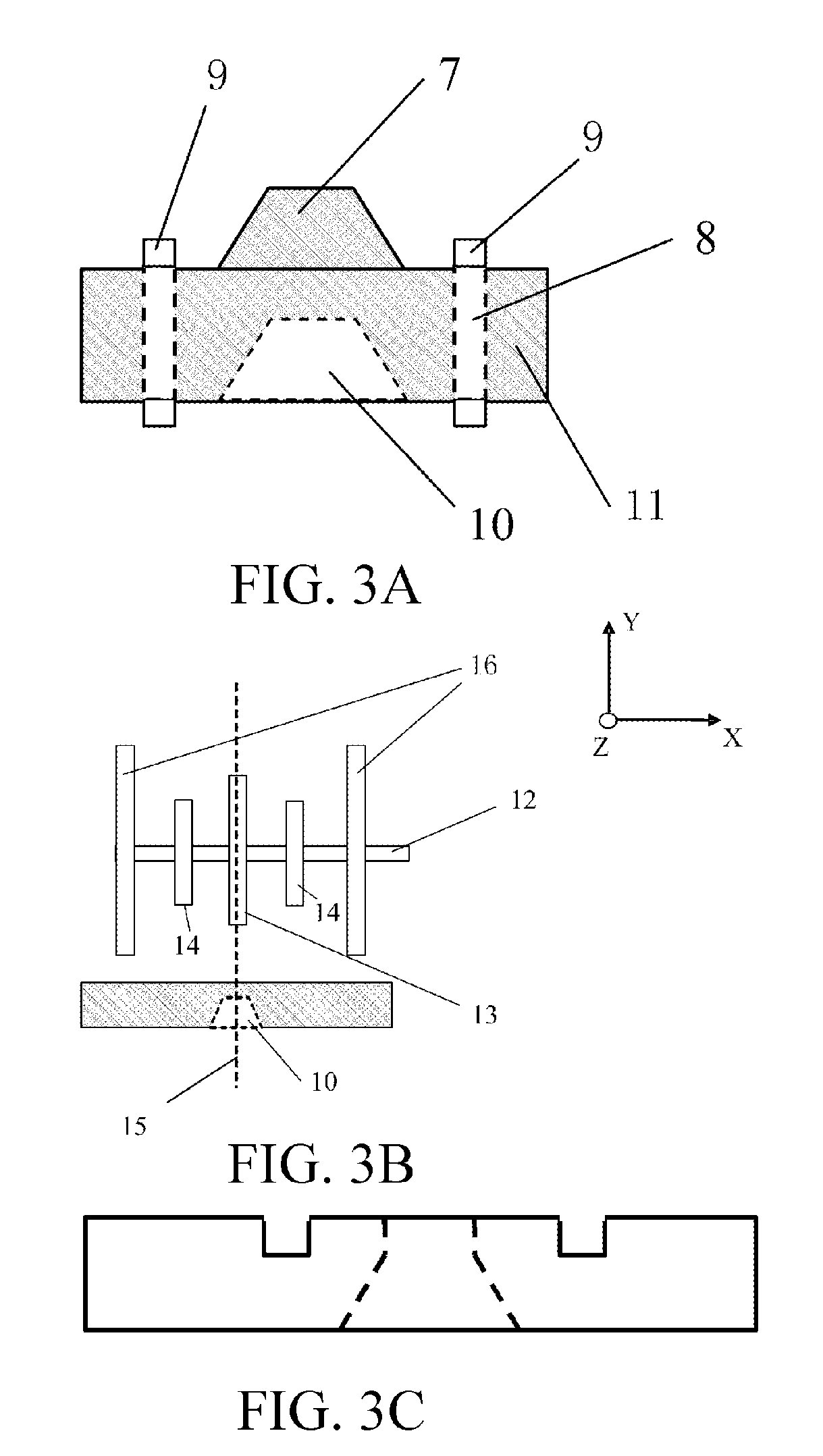
[0036]As shown in FIG. 3A, first, it is necessary to press the raw material, that is, ceramic powder, with a mold, and the mold may be used to embed an extraction groove 10 for ion extraction into a ceramic substrate 11; two thin metal rods 9 are also embedded into the substrate 11 for forming a through hole 8 for conducting upper and lower surface electrodes of the ceramic. To counteract stress, a protrusion 7 on the substrate surface is specifically designed. The whole substrate, upon completion of pressing, is fed into a high-temperature furnace, initial sintering is performed for 0.5-1.0 hours in an environment of 900-1000, the initially sintered ceramic sheet is taken out after the furnace temperature is reduced to the room temperature, and finishing is performed on the...
second embodiment
[0045]1. Prepare a Substrate
[0046]In this embodiment, glass is selected, for example, borosilicate glass or phosphosilicate glass is used as a substrate material to be machined. Moreover, glass is compounded with silicon to form a complete substrate. Herein, a thicker glass layer, as a material with higher strength, can provide support for the substrate. A silicon wafer is suitable for cutting. In an embodiment, the mature electrostatic bonding process in a micro-electromechanical system (MEMS) is used to prepare the compound substrate.
[0047]Before the bonding process, it is necessary to process a glass substrate 23, mainly including preparing metal layers 24, 25 and 27 used as electrode leads on a part of the surface and s side of the glass substrate 23; as the bonding depth is only a few microns, the thickness of the prepared electrode is controlled between hundreds of nanometers to 1 micron, and it is required that a stronger binding force exists between the prepared electrodes 2...
PUM
| Property | Measurement | Unit |
|---|---|---|
| Thickness | aaaaa | aaaaa |
| Ratio | aaaaa | aaaaa |
| Electrical conductor | aaaaa | aaaaa |
Abstract
Description
Claims
Application Information


