System and a method for designing a hybrid memory cellwith memristor and complementary metal-oxide semiconductor

a technology of complementary metal-oxide semiconductor and memory cell, which is applied in the field of memory devices, can solve the problems of many new design challenges, the progress of utilizing other emerging magnetic-based memory technologies, and the main memory of high density features also faces challenges, so as to minimize the drift of state and minimize the drift

Active Publication Date: 2014-06-05
KHALIFA UNIV OF SCI & TECH
View PDF1 Cites 25 Cited by
  • Summary
  • Abstract
  • Description
  • Claims
  • Application Information

AI Technical Summary

Benefits of technology

[0026]According to an embodiment herein, a plurality of hybrid non-volatile memory cells are designed to provide a hybrid memory architecture. The hybrid memory architecture prevents a leakage of a power during a data storage. The hybrid memory array architecture controls a drifting of a read state during a read access.
[0029]According to an embodiment herein, the control logic uses the read and write logic to minimize an instability of a data stored in the hybrid non-volatile memory cells. A direction of a read current is selected to incur minimum impact on a state drift.
[0034]According to an embodiment herein, the control logic minimizes a state drift during a read operation from the hybrid non-volatile memory cell. The state drift is minimized by reading the data with a decaying voltage. A direction of read is from OFF state to ON state.

Problems solved by technology

However, a technology scaling which enables a packing of 100's of millions of transistors on a same die brings many new design challenges due to an increase in a leakage and variability combined with the requirements for a low voltage supply operation.
The currently available main stream / CMOS-based memory technologies such as Static Random Access Memory (SRAM), Dynamic Random Access Memory (DRAM), Flash, face many challenges in a pursuit to meet an increasing demand for a quick / faster processing and for a larger data size due to the scaling limitations both in terms of an area and a voltage.
While DRAM which used as a main memory for its high density features also faces challenges due to a voltage scaling requiring an increased cell capacitance.
The challenges in the Flash memory are in a cell to cell interface in closely packed cell and a stress-induced leakage current due to a programming with a high voltage across an ultra-thin oxide.
In addition to the above, the progress in utilizing the other emerging magnetic-based memory technologies such as embedded Dynamic Random Access Memory (eDRAM), Magneto-Resistive Random Access Memory (MRAM), and Phase Change Random Access Memory (PCRAM), is hindered by a lack of compatibility with the CMOS devices, a slow access time, a temperature sensitivity and a limited scalability.
A Phase Change Random Access Memory (PCRAM) has been investigated for long time but a requirement of high voltage to cause a phase change in PCRAM makes the PCRAM less attractive for the low power applications.
Such a design faces many challenges as it is relatively new and it is not highly compatible with an existing fabrication technology.
Also, the crossbar arrays were shown to suffer from the existence of sneak paths in which a stored data at one cross-point (junction) can be easily misread.
However, Simulation Program with Integrated Circuit Emphasis (SPICE) simulations for such memory shows that the memristor state is not stable under a continuous reading.
Also, a high level architecture for such memory was not designed.
The eDRAM is found to be less attractive due to a slower access time, a need for refreshes, and an added cost due to additional masks needed to realize the added capacitor.
Other Magnetic based memory like MRAM has also been investigated but its adaption has not been successful due to its bigger area and a limited scaling in addition to a slow access time.

Method used


Image

  • System and a method for designing a hybrid memory cellwith memristor and complementary metal-oxide semiconductor
  • System and a method for designing a hybrid memory cellwith memristor and complementary metal-oxide semiconductor
  • System and a method for designing a hybrid memory cellwith memristor and complementary metal-oxide semiconductor

Examples


Embodiment Construction

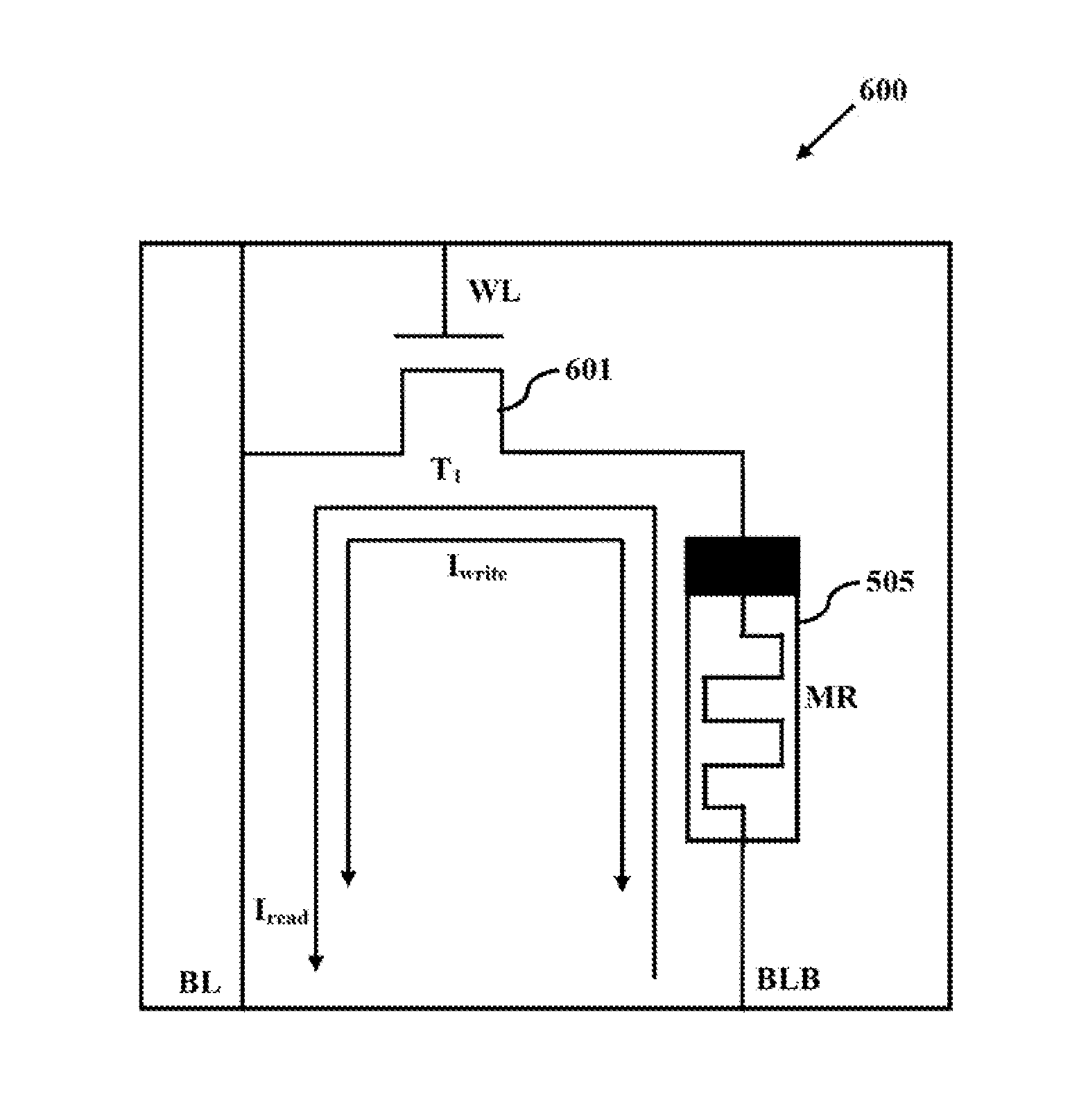
[0015]The primary object of the embodiments herein is to provide a method and a system for designing an improved hybrid memory cell and a hybrid memory array architecture using a memristor and a CMOS technology.

[0016]Another object of the embodiments herein is to provide a method and a system to integrate a memristor to the existing integrated circuits (ICs) technologies for an efficient operation.

[0017]Yet another object of the embodiments herein is to provide a hybrid memory cell of memristor and CMOS devices with a high density and a low overall power consumption characteristics.

[0018]Yet another object of the embodiments herein is to provide a control logic for a read and write operation for maximizing an efficiency of a memory cell with a low power consumption.

[0019]These and other objects and advantages of the embodiments herein will become readily apparent from the following detailed description taken in conjunction with the accompanying drawings.

SUMMARY

[0020]The various embo...


PUM


Abstract

The embodiments herein relates to a hybrid non-volatile memory cell system and architecture for designing integrated circuits. The system comprises CMOS access transistor connected to a memristor which stores a data based on a resistance. The system has a word line for accessing the hybrid memory and two bit lines carrying data of mutually opposite values for transferring a data from the memory. The two terminals of the transistor are connected respectively to a first terminal of the memristor and to a first bit line. The gate terminals of the transistors are coupled together to form a word line. The access transistors control the two bit lines during a read and write operation. A control logic performs a read and write operation with the hybrid memory cells. The memory architecture prevents a power leakage during data storage and controls a drift in a state during a read process.

Description

BACKGROUND[0001]1. Technical Field[0002]The embodiments herein generally relate to a memory device and particularly relate to Memristors based memory cells in designing integrated circuits (IC). The embodiments herein more particularly relates to a system and method for designing a hybrid memory cell with Memristor as memory element, and Complementary Metal-Oxide Semiconductor (CMOS) control logic for handling all peripheral circuits and input and output of data.[0003]2. Description of the Related Art[0004]The discovery of realizing a memristor as a physical device in 2008 spurred a great interest in using the memristors as a fundamental electronic element. The memristor based technology provides a much better scalability and a higher utilization, when used as a memory. Also, the memristor based technology provides a lower overall energy consumption compared to a traditional CMOS or Flash technology.[0005]The memristor is made of a thin film of a semiconductor oxide. The memristor i...

Claims


Application Information

Patent Timeline
Patent Type & Authority Applications(United States)
IPC IPC(8): G11C13/00
CPCG11C13/0007G11C13/0002G06F30/392G11C13/004G11C13/0069
Inventor BAKER, SHEHADAH MOHAMMADAL-HOMOUZ, DIRAR
Owner KHALIFA UNIV OF SCI & TECH
Why Eureka
Try Eureka