One-dimensional titanium nanostructure and method for fabricating the same

a titanium nanostructure and one-dimensional technology, applied in the direction of crystal growth process, polycrystalline material growth, transportation and packaging, etc., can solve the problems of high manufacturing cost, high manufacturing cost, and high manufacturing cost, and achieve the effect of reducing fabrication cost and shortening the manufacturing process

Inactive Publication Date: 2014-07-10
NAT CHIAO TUNG UNIV
View PDF3 Cites 3 Cited by
  • Summary
  • Abstract
  • Description
  • Claims
  • Application Information

AI Technical Summary

Benefits of technology

[0008]The primary objective of the present invention is to provide a to one-dimensional titanium nanostructure and a method for fabricating the same, wherein a CVD (Chemical Vapor Deposition) method is used to fabr...

Problems solved by technology

The method has disadvantages of expensive equipment and complicated processes.
Further, the wavelength of the laser limits the size of nanowires.
The metallic nanostructure fabricated by the method is likely to have many tumbling defects.
Besides, th...

Method used


Image

  • One-dimensional titanium nanostructure and method for fabricating the same
  • One-dimensional titanium nanostructure and method for fabricating the same
  • One-dimensional titanium nanostructure and method for fabricating the same

Examples


Embodiment Construction

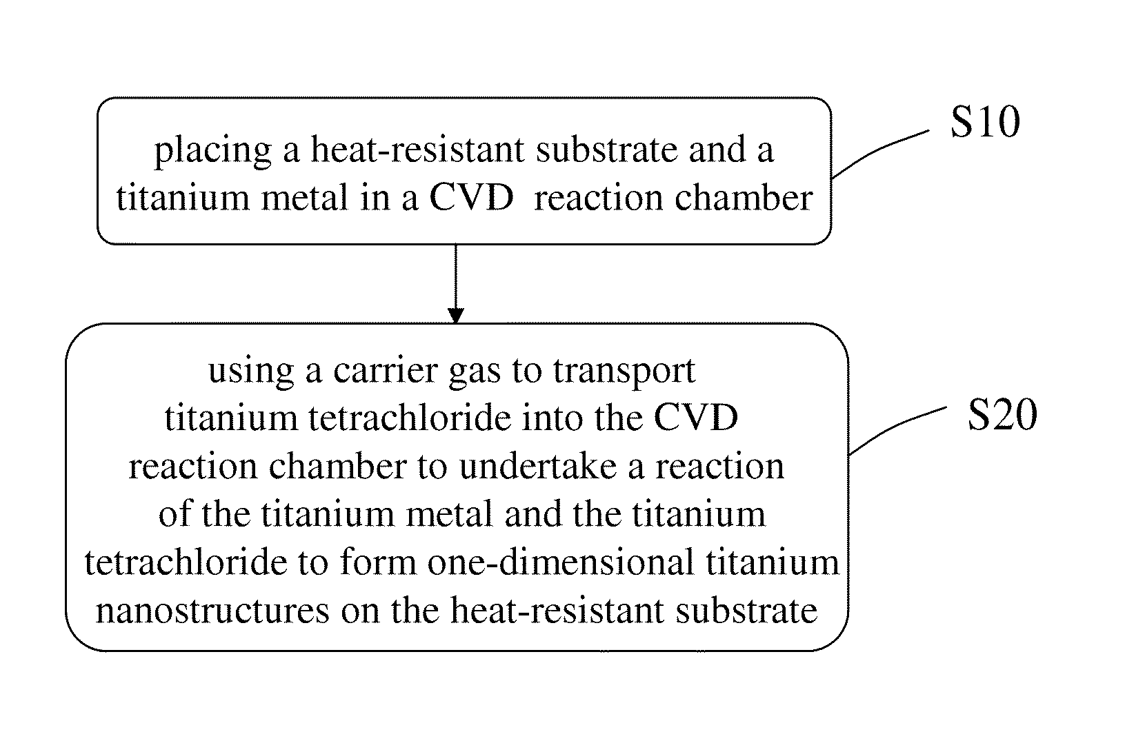
[0026]The present invention provides a method for fabricating a one-dimensional titanium nanostructure, which uses a CVD method to grow a one-dimensional titanium nanostructure. Refer to FIG. 1. The method of the present invention comprises Step S10 and Step S20.

[0027]In Step S10, respectively place a powder of a titanium metal and a heat-resistant substrate in a high temperature region and a low temperature region of a high temperature-resistant quartz tube of a CVD reaction chamber. The heat-resistant substrate may be made of any commercially-available heat-resistant material, such as graphite. The high temperature region and the low temperature region are respectively the region where the titanium metal reacts with titanium tetrachloride and the region where the product is generated. The temperature of the high temperature region and the temperature of the low temperature region are respectively referred to as the reaction temperature and the deposition temperature.

[0028]In Step ...


PUM

PropertyMeasurementUnit
Temperatureaaaaaaaaaa

Abstract

A one-dimensional titanium nanostructure and a method for fabricating the same are provided. A titanium metal reacts with titanium tetrachloride to form the one-dimensional titanium nanostructure on a heat-resistant substrate in a CVD method and under a reaction condition of a reaction temperature of 300-900° C., a deposition temperature of 200-850° C., a flow rate of the carrier gas of 0.1-50 sccm and a reaction time of 5-60 hours. The titanium nanostructure includes titanium nanowires, titanium nanobelts, flower-shaped titanium nanowires, titanium nanorods, titanium nanotubes, and titanium-titanium dioxide core-shell structures. The titanium nanostructure can be densely and uniformly grown on the heat-resistant substrate. The present invention neither uses a template nor uses the complicated photolithographic process, solution preparation process, and mixing-coating process. Therefore, the process scale-up, cost down, and the simplified production process are achieved.

Description

BACKGROUND OF THE INVENTION[0001]1. Field of the Invention[0002]The present invention relates to a metallic nanostructure synthesis technology particularly to a one-dimensional titanium nanostructure and a method for fabricating the same.[0003]2. Description of the Related Art[0004]The current metallic nanostructure synthesis technology includes a photolithographic method, a hard template method, a seed-mediated growth method and a de-alloy method.[0005]In the photolithographic method, a layer of photoresist is coated on a substrate and illuminated by the light filtered by a photomask. The pattern of the photomask reflects incident light. The light passing the photomask has a pattern identical to the pattern of the photomask and selectively exposes the photoresist coated on the substrate, whereby the pattern of the photomask is completely duplicated to the photoresist. After the abovementioned exposing step, the exposed photoresist is developed to reproduce the pattern of the photom...

Claims


Application Information

Patent Timeline
IPC IPC(8): C23C16/44
CPCB82B1/00C30B25/005C22B34/10C30B29/60C30B29/02B22F2201/40B22F9/30C23C16/44B22F1/0025C30B29/602B22F1/0547C23C16/08C23C16/46C30B25/16
Inventor CHEN, TZE-LUNGCHIU, HSIN-TIENLEE, CHI-YOUNG
Owner NAT CHIAO TUNG UNIV
Why Eureka
Try Eureka