Charge-transporting varnish

a charge-transporting varnish and charge-transporting technology, applied in the direction of electrically-conductive paints, conductors, non-metal conductors, etc., can solve the problems of reducing the color purity and color reproducibility of organic electroluminescents, major obstacles to the stable production of organic el devices, and reducing the driving voltage. , to achieve the effect of enhancing light extraction efficiency, reducing the driving voltage and high transparency

Active Publication Date: 2014-08-14
NISSAN CHEM IND LTD
View PDF4 Cites 8 Cited by
  • Summary
  • Abstract
  • Description
  • Claims
  • Application Information

AI Technical Summary

Benefits of technology

[0015]A charge-transporting thin-film whose absorption of light in the visible wavelength spectrum is suppressed and which has a high transparency can be obtained using the charge-transporting varnish of this invention. By using this thin-film, the color reproducibility of a device can be ensured without lowering the color purity of electroluminescent light or light that has passed through a color filter, markedly helping to enhance light extraction efficiency from the emission layer to the exterior and making is it possible in turn to, for example, miniaturize organic EL devices and lower their driving voltage.
[0016]By using the charge-transporting varnish of the invention, a charge-transporting thin-film endowed with a high transparency and a electrical co...

Problems solved by technology

Coloration of the charge-transporting thin-film is known to decrease the color purity and color reproducibility of an organic electroluminescent (abbreviated below as “organic EL”) device.
Moreover, such coloration is a pr...

Method used


Image

  • Charge-transporting varnish
  • Charge-transporting varnish
  • Charge-transporting varnish

Examples


synthesis example 1

[0112]The NSO-2 used in the working examples of the invention and the comparative examples was synthesized by the following reaction, based on the description provided in International Disclosure WO 2006 / 025342.

[0113]That is, 4.797 g (14.36 mol) of perfluorobiphenyl, 4.167 g (30.15 mol) of potassium carbonate and 100 mL of N,N-dimethylformamide were successively added to 11 g (31.59 mmol) of thoroughly dried sodium 1-naphthol-3,6-disulfonate, and the reaction system was flushed with nitrogen, following which the mixture was stirred for six hours at an internal temperature of 100° C.

[0114]The system was allowed to cool to room temperature, then an additional 500 mL of N,N-dimethylformamide was added and stirring at room temperature was carried out for 90 minutes so as to re-dissolve the NSO-2 that had precipitated out following the reaction. After stirring at room temperature, this solution was filtered to remove potassium carbonate residues, then concentrated under reduced pressure....
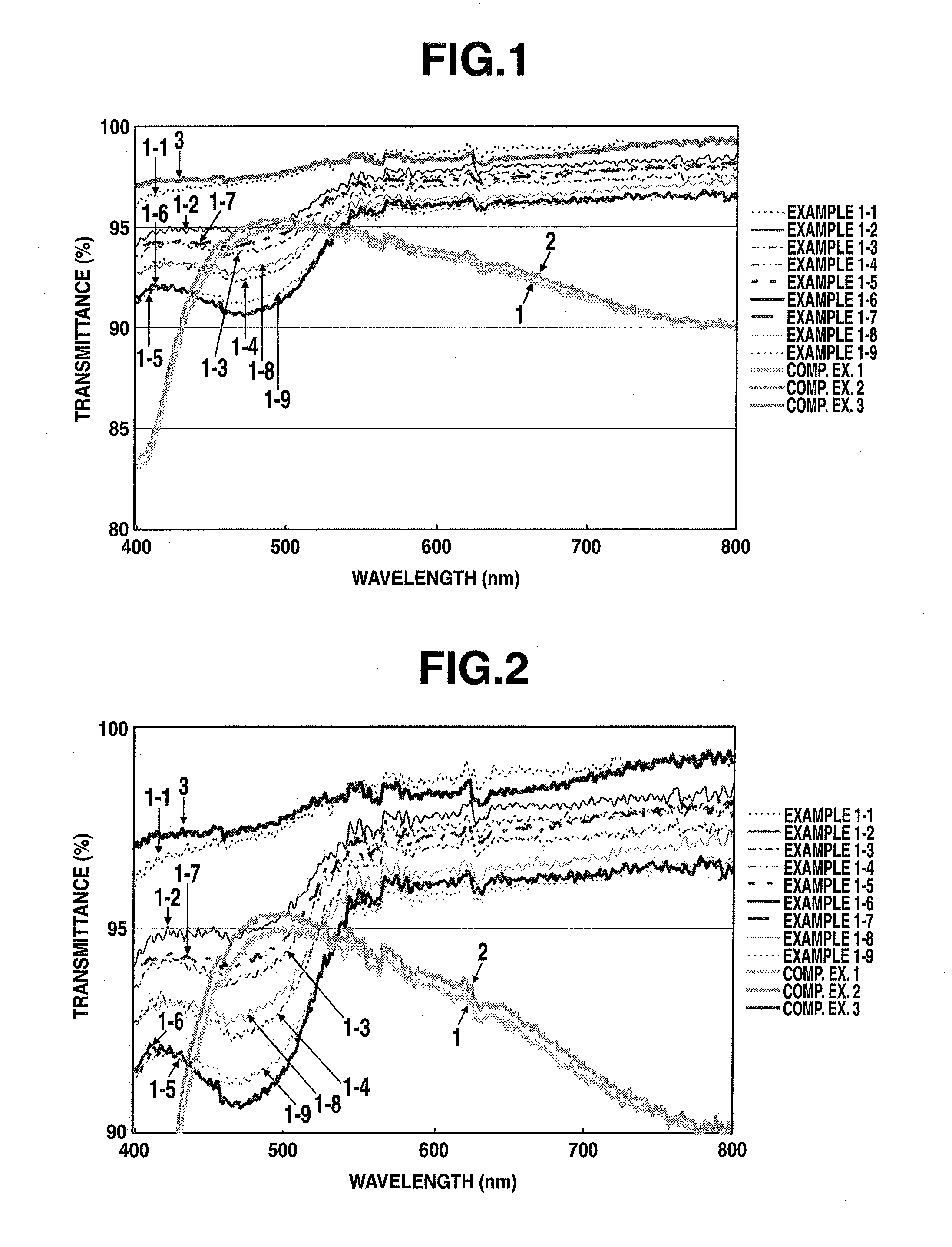
example 1-1

[0120]The N,N′-diphenylbenzidine (abbreviated below as “DPBZ”; from Tokyo Chemical Industry Co., Ltd.) of formula [1] below was recrystallized from 1,4-dioxane, then thoroughly dried in vacuo. Next, 0.244 g (0.726 mmol) of the vacuum-dried DPBZ and 0.246 g (0.272 mol) of NSO-2 were dissolved in 8 g of 1,3-dimethyl-2-imidazolidinone (abbreviated below as “DMI”) under a nitrogen atmosphere. Then 12 g of cyclohexanol (CHA) and 4 g of propylene glycol (PG) were added to the resulting solution, followed by stirring, thereby preparing a charge-transporting varnish (solids content, 2.0 wt %).

[0121]The resulting varnish was coated onto a quartz substrate with a spin coater, then dried at 50° C. for 5 minutes in open air and baked at 230° C. for 15 minutes, thereby forming a uniform thin-film having a thickness of 30 nm on the quartz substrate.

[0122]Here and in the examples that follow, quartz substrates were used after removing impurities on the surface with a plasma cleaning system (150 W,...

example 1-2

[0123]Aside from setting the amount of DPBZ used to 0.163 g (0.485 mmol) and using 0.229 g (0.253 mmol) of NSO-2 and 0.098 g (0.034 mmol) of phosphotungstic acid (Kanto Chemical Co., Ltd.) instead of 0.246 g of NSO-2, a uniform thin-film having a thickness of 30 nm was formed on a quartz substrate by the same method as in Example 1-1.


PUM

PropertyMeasurementUnit
Electric chargeaaaaaaaaaa
Transparencyaaaaaaaaaa

Abstract

This charge-transporting varnish, which contains a solvent, an electron-accepting dopant substance, and an aryldiamine compound represented by formula (1), imparts a charge-transporting thin film that has high transparency and can evince favorable element characteristics when applied to an organic EL element.
(In the formula: R1-R4 each independently represent a hydrogen atom, a halogen atom, a nitro group, a cyano group, a hydroxyl group, a thiol group, a phosphate group, a sulfone group, a carboxyl group, an alkoxy group having 1-20 carbon atoms, or the like; R5-R8 each independently represent a hydrogen atom, a phenyl group, a naphthyl group, a pyridyl group, a pyrimidinyl group, a pyridazinyl group, a pyrazinyl group, a furanyl group, a pyrrolyl group, a pyrazolyl group, an imidazolyl group, a thienyl group, or the like; and n represents an integer from 2 to 5.)

Description

TECHNICAL FIELD[0001]The present invention relates to a charge-transporting varnish. More specifically, the invention relates to a charge-transporting varnish which is capable of providing an electrically conductive thin-film of excellent transparency.BACKGROUND ART[0002]The inventors earlier reported that a charge-transporting thin-film obtained from an organic solvent-based charge-transporting varnish which contains a charge-transporting material composed of a low-molecular-weight oligoaniline compound exhibits excellent electroluminescent device characteristics (see Patent Document 1).[0003]In the charge-transporting varnish of Patent Document 1, the low-molecular-weight oligoaniline compound making up the charge-transporting material possesses within the molecule an identical repeating unit structure and has the property of becoming increasingly colored with extension of the conjugated system such that, when the varnish is rendered into a charge-transporting thin-film, light abs...

Claims


Application Information

Patent Timeline
IPC IPC(8): H01L51/00H01L51/50C09D5/24C09D7/63
CPCC09D5/24H01L51/0021H01L51/0059H01L51/5088H01L51/5056C08K5/42C08K5/18H10K85/631H10K50/17H10K50/841C09D7/63H10K50/00H10K50/15H10K50/84H10K71/60
Inventor NAKAIE, NAOKIHIROI, YOSHIOMIHOSHINO, MINORU
Owner NISSAN CHEM IND LTD
Why Eureka
Try Eureka