Quantum cascade laser

a laser and quantum cascade technology, applied in the direction of laser details, laser optical resonator construction, semiconductor lasers, etc., can solve the problems of difficult to change the emission wavelength in a wide wavelength range, difficult to realize a broad gain spectrum, and heat generated in the central region of the qcl device is not easily dissipated, etc., to achieve good characteristics, low absorption coefficient, and high resistance to electrons

Active Publication Date: 2014-12-04
SUMITOMO ELECTRIC IND LTD
View PDF9 Cites 7 Cited by
  • Summary
  • Abstract
  • Description
  • Claims
  • Application Information

AI Technical Summary

Benefits of technology

[0018]In the quantum cascade laser according to the present invention, the current blocking layer may be formed of a semi-insulating semiconductor. In addition, the current blocking layer may be formed of InP or AlInAs doped with at least one of Fe, Ti, Cr, and Co. Since a semi-insulating semiconductor has high resistance to electrons, the semi-insulating semiconductor is suitable for constituting the current blocking layer. In addition, a semi-insulating semiconductor has a low absorption coefficient for light having a mid-infrared wavelength. Therefore, even when the current blocking layer formed of such a semi-insulating semiconductor is introduced, good characteristics are maintained. Further, a semi-insulating semiconductor has high thermal conductivity. When such a semi-insulating semiconductor is used in the current blocking layer, the heat dissipation of the QCL device is improved, so that high-temperature operations are possible.
[0019]In the quantum cascade laser according to the present invention, the buried region may be formed of a semi-insulating semiconductor. In addition, the buried region may be formed of InP or AlInAs doped with at least one of Fe, Ti, Cr, and Co. Since a semi-insulating semiconductor has high resistance to electrons and high thermal conductivity, the semi-insulating semiconductor is suitable for constituting the buried regions. In addition, a semi-insulating semiconductor has a low absorption coefficient for light having a mid-infrared wavelength. Therefore, even when the buried region formed of such a semi-insulating semiconductor is introduced, a waveguide loss is not increased, so that good characteristics are maintained.

Problems solved by technology

Therefore, in QCLs having a divided-core structure, it is difficult to realize a broad gain spectrum.
Therefore, heat generated at the core region in the central portion of the QCL device is not easily dissipated.
In a QCL having such a gain spectrum of a narrow bandwidth, it is difficult to change an emission wavelength in a wide wavelength range.
Therefore, in divided-core structures having a uniform width of the core regions, it is difficult to realize a light source such as a tunable laser and a multi-wavelength semiconductor laser array having a wide emission wavelength band.

Method used


Image

  • Quantum cascade laser
  • Quantum cascade laser
  • Quantum cascade laser

Examples


first embodiment

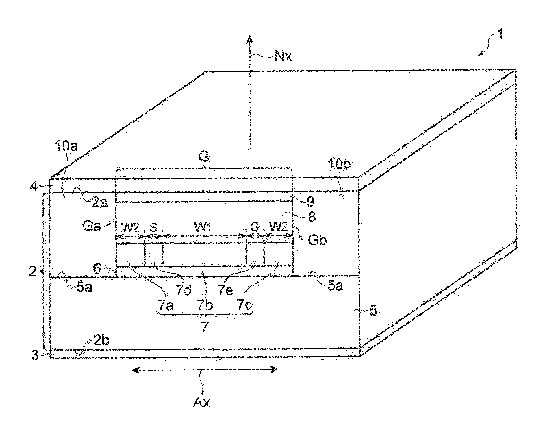
[0046]FIG. 1 illustrates a quantum cascade laser 1 according to the first embodiment. FIG. 1 illustrates an external shape of the quantum cascade laser 1 and an internal structure of the quantum cascade laser 1 in a plane that is perpendicular to a waveguide (that is, a plane defined by a normal direction Nx and a reference direction Ax described later). The quantum cascade laser 1 includes a semiconductor layer 2, a lower electrode 3, and an upper electrode 4. The lower electrode 3 is provided on a back surface 2b of the semiconductor layer 2. The upper electrode 4 is provided on a principal surface 2a of the semiconductor layer 2. The semiconductor layer 2 of the quantum cascade laser 1 includes an n-type semiconductor substrate 5, a mesa waveguide Q a current blocking layer 10a, and a current blocking layer 10b. The mesa waveguide G is provided on a principal surface 5a of the n-type semiconductor substrate 5. The lower electrode 3 is provided on a back surface of the n-type semi...

second embodiment

[0096]In the first embodiment, the buried regions made of a semi-insulating semiconductor are formed in only the light emitting region. In the embodiment, the buried regions are extended from the light emitting region toward outside in the normal direction of the principal surface of the n-type semiconductor substrate and in a direction opposite to the normal direction so as to protrude from the light emitting region.

[0097]In a quantum cascade laser 101 shown in FIG. 6A, buried regions (buried regions 71d and 71e) are extended from a light emitting region 7 to middle portions of upper and lower cladding layers (an n-type lower cladding layer 61 and an n-type upper cladding layer 81. Alternatively, as in a quantum cascade laser 102 shown in FIG. 6B, buried regions (buried regions 72d and 72e) may be extended from a light emitting region 7 to a substrate 5 through the lower cladding layer (an n-type lower cladding layer 62) and to an n-type contact layer 9 through the upper cladding l...

third embodiment

[0104]In each of the first and second embodiments above, as a current confinement structure, the QCL device includes a BH structure including current blocking layers formed of a semi-insulating semiconductor such as Fe-doped InP. However, the current confinement structure is not limited thereto. For example, in a quantum cascade laser 105 shown in FIG. 8, an insulating film 11a and an insulating film 11b are formed on side surfaces Ga and Gb of a mesa waveguide G, respectively as the current confinement structure.

[0105]The quantum cascade laser 105 shown in FIG. 8 includes a semiconductor layer 25. The semiconductor layer 25 includes an n-type semiconductor substrate 5 and a mesa waveguide G. However, the semiconductor layer 25 does not include the current blocking layers 10a and 10b that the semiconductor layer 2 includes in the first embodiment. The insulating films 11a and 11b are each another example of the current blocking layer. The insulating films 11a and 11b may each be for...


PUM


Abstract

A quantum cascade laser includes a semiconductor substrate including a principal surface; a mesa waveguide disposed on the principal surface of the semiconductor substrate, the mesa waveguide including a light emitting region and an upper cladding layer disposed on the light emitting region, the mesa waveguide extending in a direction orthogonal to a reference direction; and a current blocking layer formed on a side surface of the mesa waveguide. The light emitting region includes a plurality of core regions and a plurality of buried regions. The core regions and the buried regions are alternately arranged in the reference direction. The core region at a central portion of the mesa waveguide has a width larger than a width of the core region at a peripheral portion of the mesa waveguide in the reference direction.

Description

BACKGROUND OF THE INVENTION[0001]1. Field of the Invention[0002]The present invention relates to a quantum cascade laser.[0003]2. Description of the Related Art[0004]A quantum cascade laser (QCL) emits light of a mid-infrared wavelength range of approximately 3 μm to 20 μm. (A quantum cascade laser may hereunder be referred to as “QCL”.) Light of the mid-infrared wavelength range is used in environmental gas analysis, medical diagnosis, and industrial processing. Therefore, a quantum cascade laser is used in these fields. In particular, a quantum well cascade laser is small, has high-speed characteristics, and is low in cost. Therefore, the quantum well cascade laser is promising as a light source of the mid-infrared wavelength range. As an exemplary structure of such a QCL, a multi-core structure (divided-core structure) in which a core region of the QCL is divided into a plurality of tiny regions is proposed. Such a QCL is described in, for example, “Applied Physics Letters, vol. ...

Claims


Application Information

Patent Timeline
Patent Type & Authority Applications(United States)
IPC IPC(8): H01S5/34H01S5/343H01S5/12
CPCH01S5/3401B82Y20/00H01S5/34313H01S5/12H01S5/2275H01S5/3402H01S5/4031H01S5/4068H01S5/4087H01S5/2213H01S5/2224
Inventor HASHIMOTO, JUN-ICHIMURATA, MICHIO
Owner SUMITOMO ELECTRIC IND LTD
Why Eureka
Try Eureka