Substrate with transparent electrode and method for manufacturing same

a technology of transparent electrodes and substrates, which is applied in the direction of sustainable manufacturing/processing, instruments, and final product manufacturing, etc., can solve the problems of affecting the design of devices, the temperature of deposition cannot be increased in view of the heat resistance of the base material, and the film base material may undergo a dimensional change, etc., to achieve excellent productivity, improve the response speed of the capacitance touch panel, and simplify the step

Inactive Publication Date: 2014-12-18
KANEKA CORP
View PDF3 Cites 10 Cited by
  • Summary
  • Abstract
  • Description
  • Claims
  • Application Information

AI Technical Summary

Benefits of technology

[0018]According to the present invention, a substrate with a transparent electrode, which includes an amorphous transparent electrode layer having specific characteristics, is obtained. Although the amorphous transparent electrode layer is not heated at a high temperature, indium oxide that forms the transparent electrode layer is crystallized. Thus, the substrate with a transparent electrode according to the present invention can simplify a step of crystallizing a transparent electrode layer, and is therefore excellent in productivity. Further, the substrate with a transparent electrode accordin

Problems solved by technology

On the other hand, when a film is used as the transparent base material, the deposition temperature cannot be increased in view of the heat resistance of the base material.
However, heating for crystallization is required to be performed at a high temperature of about 150° C., and therefore the film base material may undergo a dimensional change and disrupt the design of a device.
Further, crystallization requires heating for about 30 minutes to several days.
Accordingly, formation of an amorphous conductive oxide thin film on the film base material is performed by the roll-to-roll method, whereas crystallization of a conductive oxide thin film is unfit for the roll-to-roll method, and is generally performed with the film cut into a predetermined size.
Thus, necessity of crystallization of a conductive oxide thin film a

Method used


Image

  • Substrate with transparent electrode and method for manufacturing same
  • Substrate with transparent electrode and method for manufacturing same

Examples


example 1

Preparation of Transparent Film Base Material

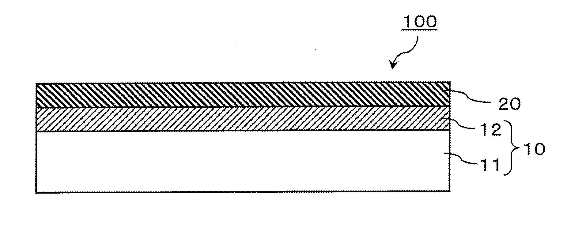
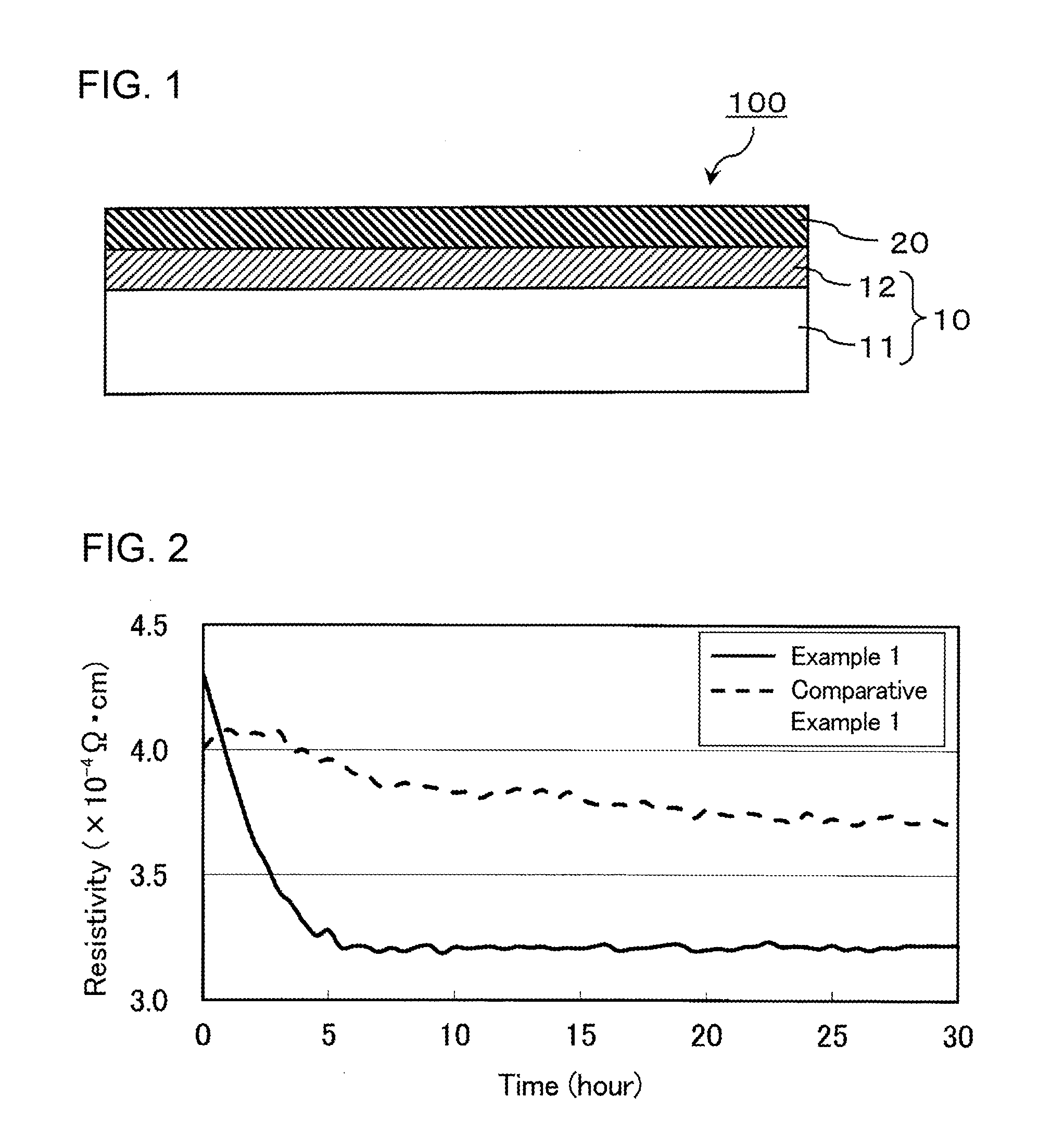
[0084]As a transparent film, a 188 μm-thick, biaxially stretched PET film provided with a hard coat layer made of a urethane-based resin formed on both surfaces thereof (heat shrinkage start temperature: 85° C.; heat shrinkage percentage during heating at 150° C. for 30 minutes: 0.6%) was used. A 40 nm-thick transparent dielectric material electrode layer made of silicon oxide (SiO2) was formed on one of the surfaces of the PET film by the sputtering method.

[0085](Deposition of Amorphous Transparent Electrode Layer)

[0086]Using indium tin oxide (content of tin oxide: 5% by weight) as a target, sputtering was performed under conditions of an oxygen partial pressure of 5×10⁻³ Pa, a deposition chamber internal pressure of 0.5 Pa, a substrate temperature of 0° C., and a power density of 4 W / cm2 while a mixed gas of oxygen and argon was introduced into the chamber. The thickness of the obtained ITO layer was 25 nm.

[0087]The substrate with a tra...


PUM

PropertyMeasurementUnit
Temperatureaaaaaaaaaa

Abstract

The present invention relates to a substrate with a transparent electrode, which has a transparent electrode layer on at least one surface of a transparent film base material. The transparent film base material has a transparent dielectric material layer containing an oxide as a main component on a surface at the transparent electrode layer side. In one embodiment of the present invention, the transparent electrode layer is a crystalline transparent electrode layer that has a crystallinity degree of 80% or more. In this embodiment, the crystalline transparent electrode layer has a resistivity of 3.5×10⁻⁴ Ω·cm or less, a thickness of 15 nm to 40 nm, an indium oxide content of 87.5% to 95.5%, and a carrier density of 4×10²⁰/cm3 to 9×10²⁰/cm3, and the substrate with the transparent electrode preferably has a heat shrinkage start temperature of 75° C. to 120° C. as measured by thermomechanical analysis.

Description

TECHNICAL FIELD[0001]The present invention relates to a substrate with a transparent electrode, in which a transparent electrode layer is formed on a transparent film base material, and a method for manufacturing same.BACKGROUND ART[0002]A substrate with a transparent electrode, in which a conductive oxide thin film such as that of an indium-tin composite oxide (ITO) is formed on a transparent base material such as a transparent film or glass, is widely used as a transparent electrode of a display, a light emitting element, a photoelectric conversion element, or the like. As a method for manufacturing such a substrate with a transparent electrode, a method is widely used in which a conductive oxide thin film is formed on a transparent base material by the sputtering method. Preferably, the conductive oxide to be used for the transparent electrode is crystallized from the viewpoints of improving the transmittance and suppressing a change in resistance value.[0003]When a heat-resistan...

Claims


Application Information

Patent Timeline
IPC IPC(8): H05K1/02C23C14/58C23C14/34H05K1/09
CPCH05K1/0274H05K1/092H05K2201/0329C23C14/3407C23C14/5806C23C14/086C23C14/10C23C14/3414H01L31/022475H01L31/1884G06F2203/04103Y02E10/549Y10T428/265Y02P70/50G06F3/044H10K30/82H10K50/816H10K50/828H10K2102/102H10K2102/103G06F3/041G06F3/0443
Inventor KUCHIYAMA, TAKASHIHAYAKAWA, HIRONORIUEDA, HIROAKIFUJIMOTO, TAKAHISAYAMAMOTO, KENJI
Owner KANEKA CORP
Why Eureka
Try Eureka