Photovoltaic thin-film solar modules and method for manufacturing such thin-film solar modules

a technology of solar modules and solar cells, which is applied in the manufacture of final products, pv power plants, basic electric elements, etc., can solve the problems of unreasonably high manufacturing costs, difficult or impossible to manufacture thin-film solar modules on a large scale, and inability to exclude components, dopants, or impurities

Inactive Publication Date: 2015-03-12
ROBERT BOSCH GMBH
View PDF11 Cites 19 Cited by
  • Summary
  • Abstract
  • Description
  • Claims
  • Application Information

AI Technical Summary

Benefits of technology

[0015]It may also be provided that the barrier layer represents a barrier for in particular diffusing or diffusible components, in particular dopants, which migrate out of and / or through the back electrode layer, and / or for in particular diffusing or diffusible components, in particular dopants, which migrate out of and / or through the contact layer, in particular a bidirectional barrier layer. In the latter case, the barrier layer prevents the depletion from the semiconductor layer of dopant, such as sodium, which forms this layer, as the result of which an unimpaired efficiency may be maintained.
[0083]It has also proven to be advantageous to have multiple method steps carried out in a single unit. This applies, for example, to the first and second structuring steps and the filling of the first structuring separating trench with an insulator material. The method according to the present invention thus allows more cost-effective processing with a marked improvement in performance. In addition, the semiconductor absorber layer may be provided with dopants in a much more targeted manner.

Problems solved by technology

Due to plant engineering constraints, it is often extremely difficult or impossible to manufacture thin-film solar modules on a large scale having a module format with a size greater than 1.2 m×0.5 m. In addition, for the temperatures and reaction conditions to be used in the individual manufacturing stages, it has not been possible thus far to exclude contamination or interdiffusion of components, dopants, or impurities of individual layers of the multilayer system.
Although it is possible to achieve good efficiencies by using particularly pure back electrode material, this is generally accompanied by unreasonably high manufacturing costs.
In addition, the above-mentioned phenomena of migration and in particular diffusion under the customary manufacturing conditions quite often result in significant contamination of the back electrode material.
Even when attention is paid to optimizing all methods and materials, one is always greatly limited in the ultimate design of the thin-film solar modules provided for sale.
On the other hand, the barrier property for dopants which are diffusible or diffusing from the semiconductor absorber should prevent dopant thus being lost at the bulk back electrode and thus depleting the semiconductor absorber of dopant, which would greatly reduce the efficiency of the solar cell or the solar module.
It is known that these chalcogenide compounds, such as MoSe, contribute to a significant increase in volume of the layer of the back electrode near the surface, which in turn results in unevennesses in the layer structure and impaired adhesion.
This results in layer infiltration and the formation of microcracks due to mechanical stress caused by the volume expansion of the metals which are corroded under the effect of selenium and / or sulfur.
Such a melting edge is generally particularly susceptible to a reaction with selenium and / or sulfur under the conditions for forming the semiconductor absorber layer.
A pronounced volume expansion resulting in microcracks often cannot be prevented.

Method used


Image

  • Photovoltaic thin-film solar modules and method for manufacturing such thin-film solar modules
  • Photovoltaic thin-film solar modules and method for manufacturing such thin-film solar modules
  • Photovoltaic thin-film solar modules and method for manufacturing such thin-film solar modules

Examples


Embodiment Construction

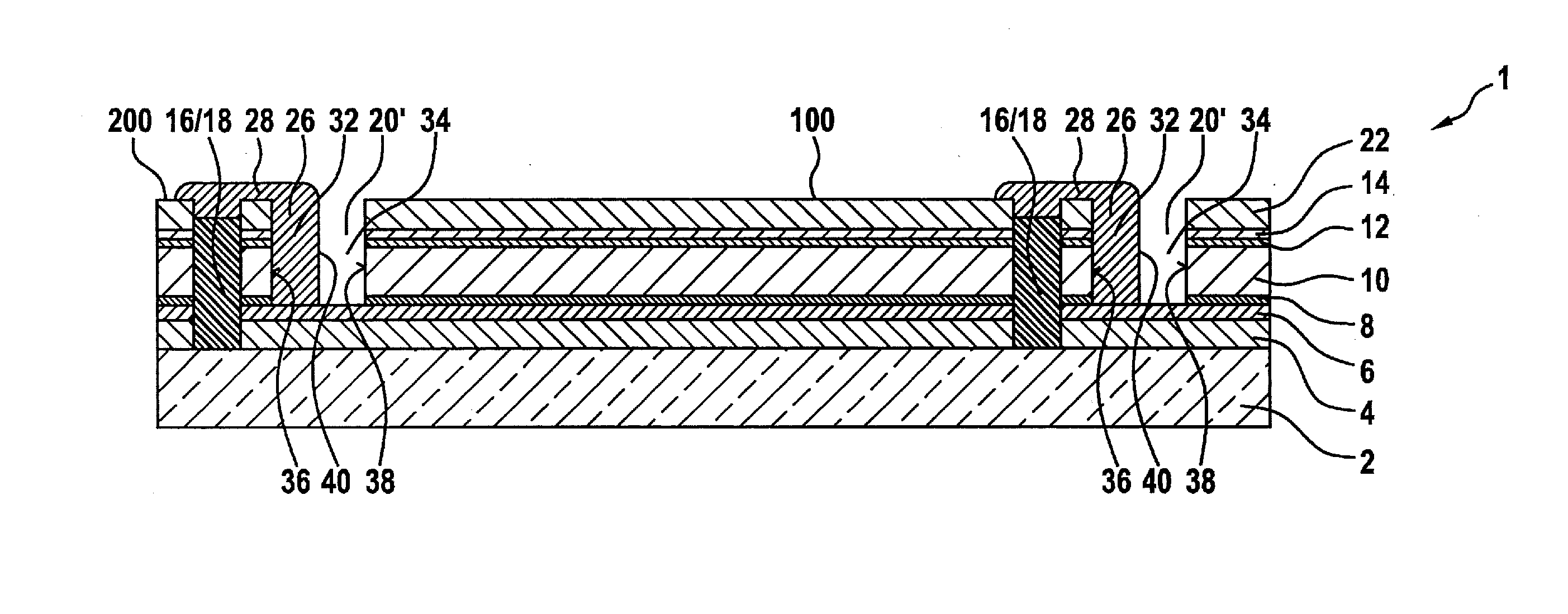
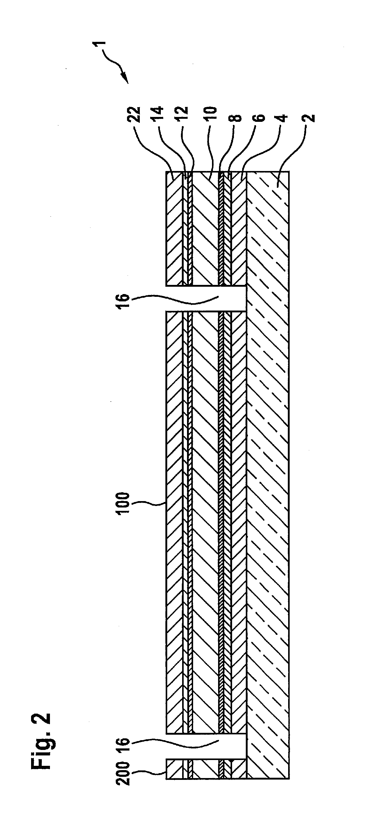
[0095]FIG. 1 shows a schematic cross-sectional view of an intermediate manufacturing stage 1a of a thin-film solar module 1 according to the present invention. A bulk back electrode layer 4 made of molybdenum, for example, with the aid of thin-film deposition is present on glass substrate 2. The bulk back electrode layer is adjoined by a bidirectional reflective barrier layer 6 made of TiN or ZrN, for example, which likewise may be obtained with the aid of thin-film deposition. In the illustrated specific embodiment, an ohmic contact layer 8 made of a metal chalcogenide such as molybdenum selenide is situated on barrier layer 6. This contact layer may be obtained in various ways, as explained above in a general way. In one embodiment, for example, molybdenum selenide from a molybdenum selenide target has been sputtered on. Alternatively, initially a metal layer may be applied which is subsequently converted into the corresponding metal chalcogenide prior to and / or during the formati...


PUM


Abstract

A photovoltaic thin-film solar module includes in the following sequence: a substrate layer; a back electrode layer directly adjoining the substrate layer; a conductive barrier layer directly adjoining at least one of the back electrode layer and the substrate layer; an ohmic contact layer directly adjoining the barrier layer; one of a chalcopyrite or kesterite semiconductor absorber layer directly adjoining the contact layer; a first buffer layer directly adjoining the semiconductor absorber layer and containing one of Zn(S,OH) or In2S3; a second buffer layer directly adjoining one of the semiconductor absorber layer or the first buffer layer; and a transparent front electrode layer directly adjoining at least one of the semiconductor absorber layer, the first buffer layer, and the second buffer layer, the transparent front electrode layer containing n-doped zinc oxide.

Description

BACKGROUND OF THE INVENTION[0001]1. Field of the Invention[0002]The present invention relates to photovoltaic thin-film solar modules and a method for manufacturing such thin-film solar modules.[0003]2. Description of the Related Art[0004]Photovoltaic solar modules have been known and also commercially available for quite some time. Suitable solar modules include, on the one hand, crystalline, amorphous silicon solar modules, and on the other hand, so-called thin-film solar modules. These types of thin-film solar modules are based, for example, on the use of a so-called chalcopyrite semiconductor absorber layer, such as a Cu(In,Ga) (Se,S) system, and represent a complex multilayer system. In these thin-film solar modules, a molybdenum back electrode layer usually rests on a glass substrate. In one method variant, the molybdenum back electrode layer is provided with a precursor thin metal layer containing copper, indium, and optionally gallium, and is subsequently converted into a so...

Claims


Application Information

Patent Timeline
Patent Type & Authority Applications(United States)
IPC IPC(8): H01L31/0224H01L31/18H01L31/05H01L31/032H01L31/0475
CPCH01L31/022441H01L31/022483H01L31/0323H01L31/1828H01L31/0475H01L31/0508H01L31/0327H01L31/0326H01L31/03923H01L31/0749H01L31/0465Y02E10/541Y02E10/543Y02P70/50
Inventor PROBST, VOLKER
Owner ROBERT BOSCH GMBH
Why Eureka
Try Eureka