Method for the deposition of an organic material

a technology of organic materials and methods, applied in the direction of diketopyrrolopyrrole dyes, naphthalimide/phthalimide dyes, thermoelectric devices, etc., can solve the problems of increasing production times, increasing costs, and increasing costs on an industrial scal

Active Publication Date: 2015-05-07
CLAP CO LTD
View PDF11 Cites 15 Cited by
  • Summary
  • Abstract
  • Description
  • Claims
  • Application Information

AI Technical Summary

Benefits of technology

[0066]It has surprisingly been found that the method of the present invention yields high-quality polycrystalline films on a wide variety of supports in an atmosphere which is at ambient pressure or an atmosphere which is at a pressure close to ambient pressure, without having to resort to costly high-vacuum techniques of prior art physical vapor deposition processes. For instance, organic semiconducting layers produced with the method of the present invention, yield high charge carrier mobilities, e.g. of up to 0.9 cm2 / Vs, and high on / off ratios, e.g. of more than 1×10⁵. Such layers can, for example, be employed advantageously to produce organic field effect transistors. Furthermore, organic semiconducting layers produced with the method of the present invention show an remarkably improved storage stability over layers produced with the conventional vacuum deposition method.
[0322]In a specific embodiment of the present invention, the donor-acceptor-heterojunction is in the form of a gradient bulk heterojunction. In the mixed layers composed of donor and acceptor materials, the donor-acceptor ratio changes gradually. The form of the gradient may be stepwise or linear. In the case of a stepwise gradient, the layer 01 consists, for example, of 100% donor material, layer 02 has a donor / acceptor ratio>1, layer 03 has a donor / acceptor ratio=1, layer 04 has a donor / acceptor ratio<1, and layer 05 consists of 100% acceptor material. In the case of a linear gradient, layer 01 consists, for example, of 100% donor material, layer 02 has a decreasing ratio of donor / acceptor, i.e. the proportion of donor material decreases in a linear manner in the direction of layer 03, and layer 03 consists of 100% acceptor material. The different donor-acceptor ratios can be controlled by means of the deposition rate of each and every material. Such structures can promote the percolation path for charges.

Problems solved by technology

The primary drawbacks are that theses techniques require sophisticated instrumentation and that the establishment of a high vacuum prior to deposition leads to increased production times so that these methods are rather costly on an industrial scale.
These techniques are costly because the deposition rate has to be kept rather low in order to obtain suitable single crystals and is therefore on suitable for a cheap industrial scale production process.
However, small-molecular organic semiconducting materials are difficult to dissolve in common solvents and specific solvents for individual materials which are often harmful for the environment which also increases overall production costs.
Further, spin-coating requires high viscosity solutions and is therefore usually not applicable to small molecules.
Also, organic semiconducting layers produced by coating techniques often exhibit a poor charge carrier mobility and an insufficient on / off ratio and are therefore not suitable for highly sophisticated electronic devices such as organic field-effect transistors (OFETs).

Method used


Image

  • Method for the deposition of an organic material
  • Method for the deposition of an organic material
  • Method for the deposition of an organic material

Examples


example 1

Preparation and Optical Characterization of an Organic Field-Effect Transistor (OFET)

[0348]An organic field-effect transistor (OFET) is a typical example of an organic electronic device where certain components of prior art inorganic semiconductor technology have been replaced by organic materials. In the case of an OFET, the channel of a conventional field effect transistor is made from a thin organic semiconducting layer. The thickness the organic semiconducting layer is typically below one micrometer. OFETs have been fabricated with various device geometries.

Preparation

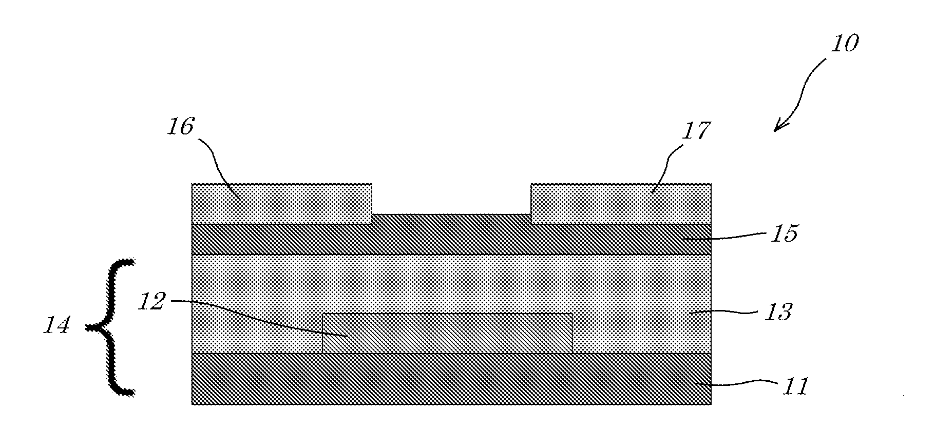
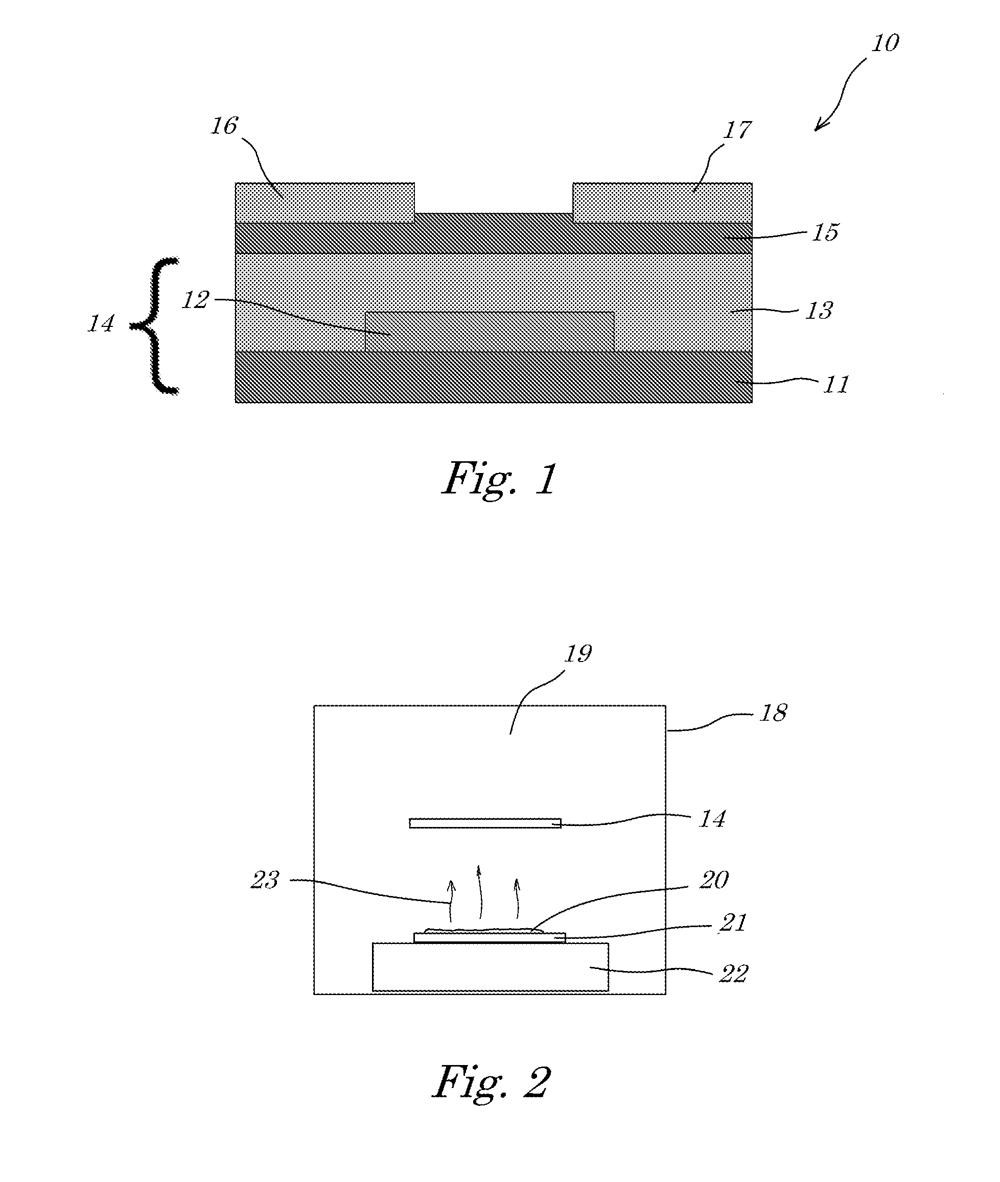
[0349]A typical example is depicted in FIG. 1 where the OFET 10 comprises a silicon wafer 11 which has been provided with metal gate electrodes 12 deposited via conventional high-vacuum physical vapor deposition techniques onto the surface of the bulk silicon 11. Subsequently an insulating dielectric layer 13 of thermally oxidized silicon has been grown. In the present case the dielectric layer 13 has a thickness o...

example 2

Preparation and Electrical Characterization of Another OFET Device

[0356]An OFET was prepared and optically characterized in accordance with Example 1 but using a different organic semiconducting material, having the following structure (B):

[0357]OFETs produced in accordance with Example 2 had a channel width (W) of 200 μm and channel length (L) of 100 μm and have been electrically characterized using an Agilent 4145C Semiconductor Parameter Analyzer.

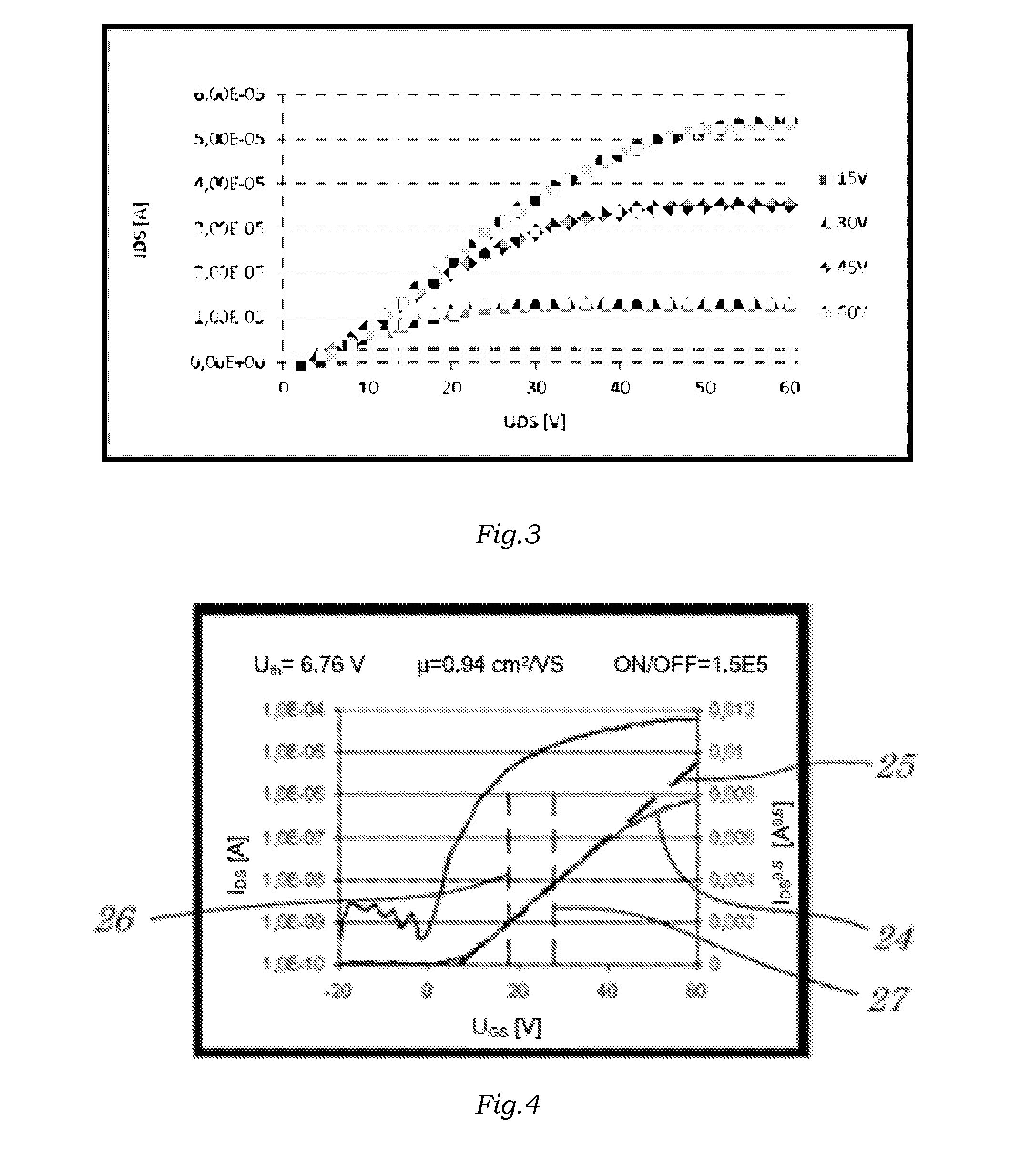
[0358]The measurement results are depicted in FIGS. 3 and 4, respectively.

[0359]FIG. 3 shows the output characteristics with UDS=0 V to +60V at 2V step size with UGS=15, 30, 45 and 60V.

[0360]FIG. 4 shows the transfer characteristics with UGS=−20 V to +60 V at 2V step size with UDS=40V

[0361]The mobility μ is calculated from the root representation of the transfer characteristic curve (reference numeral 24 in FIG. 4) calculated in the saturation region. The slope m is determined from the dashed line 25. The dashed line 25 is fitted to a re...

example 3

Electrical Characterization of an OFET Array

[0364]An organic layer of compound (B) is deposited on a wafer substrate comprising an array of 180 OFETs using the method of the present invention. In this example, the substrate is not only placed at a short distance above the heated source into the rising vapor stream but moved with constant velocity through the vapor by means of a doctor blade drawing table. This method allows to produce a very uniform and homogenous coating over a large area of the substrate surface (complete coverage of the substrate with an organic semiconducting layer having a uniform thickness). In the present example, 180 OFTs were coated and individually contacted to determine their electrical characteristics.

[0365]The measurements reveal a very good homogeneity of the transistors with nearly identical transfer characteristics. FIG. 5 is a diagram showing the transfer characteristics of the array of OFETs. Almost the same transfer characteristics is obtained for...


PUM

PropertyMeasurementUnit
pressureaaaaaaaaaa
pressureaaaaaaaaaa
pressureaaaaaaaaaa

Abstract

The present invention relates to a method for the deposition of at least one layer of an organic material on a substrate by (a) providing a source of a solid organic material in an atmosphere at a pressure comprised between 50 and 200 kPa, (b) heating said organic material to a first temperature to produce a vapor of said organic material, (c) exposing at least one surface of a substrate having a second temperature lower than said first temperature to said vapor to deposit organic material from said vapor onto said at least one surface of said substrate.

Description

FIELD OF THE INVENTION[0001]The use of organic vapor phase deposition has made progress towards the low cost, large scale deposition of small molecular weight organic layers with numerous potential applications. It is expected that, in the future, not only the classical inorganic semiconductors but increasingly also organic semiconductors based on low molecular weight or polymeric materials will be used in many sectors of the electronics industry. In many cases, these organic semiconductors have advantages over the classical inorganic semiconductors, for example better substrate compatibility and better processibility of the semiconductor components based on them. Often, organic semiconductor materials are simpler to process because they can be deposited at lower temperatures than inorganic semiconductors, allowing the use a wider range of substrate materials. For instance, they allow processing on flexible substrates such as plastic materials and enable their interface orbital ener...

Claims


Application Information

Patent Timeline
Patent Type & Authority Applications(United States)
IPC IPC(8): H01L51/00H01L51/56
CPCH01L51/001H01L51/0026H01L51/0012H01L51/0067H01L51/56H01L51/0068H01L51/0094H01L51/0077H01L51/0058C23C14/12C09B57/004C09B57/08C09B57/10Y02E10/549H10K71/00H10K71/164H10K71/40H10K71/191H10K85/30H10K85/40H10K85/626H10K85/654H10K85/655
Inventor MUSIOL, THOMASFREYBERG, DIETERBRILL, JOCHEN
Owner CLAP CO LTD
Why Eureka
Try Eureka