Organic thin film transistor, organic semiconductor thin film, and organic semiconductor material

Active Publication Date: 2015-06-18
FUJIFILM CORP
View PDF4 Cites 7 Cited by
  • Summary
  • Abstract
  • Description
  • Claims
  • Application Information

AI Technical Summary

Benefits of technology

[0037]According to the invention, a semiconductor material that has high crystallinity and forms an organic thin film advantageous for carrier transport may be provided, and thereby an organic thin film transistor that has a high carrier mobility may be provided.
[0038]According to the invention, furthermore, an organic thin

Problems solved by technology

However, it may not be said that a compound that is useful as an organic EL device material is immediately useful as a semiconductor material for an organic thin film transistor.
In general, an organic compound having high crystallinity may cause light emission defects, such as in-plane unevenness in electric field intensity, in-plane unevenness in light emission, and light emission quenching, and therefore the organic EL device material may not be enhanced in crystallinity.
Accordingly, even when an organic compound that constitutes an organic EL device is di

Method used


Image

  • Organic thin film transistor, organic semiconductor thin film, and organic semiconductor material
  • Organic thin film transistor, organic semiconductor thin film, and organic semiconductor material
  • Organic thin film transistor, organic semiconductor thin film, and organic semiconductor material

Examples


examples

[0148]The features of the invention will be described more specifically with reference to examples and comparative examples below. The materials, the amounts, the ratios, the contents of process, the procedures of process, and the like shown in the examples may be appropriately changed unless the substance of the invention is deviated. Therefore, the scope of the invention is not construed as being limited to the specific examples shown below.

synthesis example

[0149]The compounds 1 to 27 were synthesized by referring to Molecular Electronics and Bioelectronics, The Japan Society of Applied Physics, vol. 22, pp. 9-12 (2011), WO 2009 / 148016, and the like.

Production and Evaluation of Device

[0150]The materials used for producing a device were purified by sublimation, and it was confirmed that the materials had a purity of 99.5% or more with high performance liquid chromatography (Tosoh TSKgel ODS-100Z) (purity: area ratio of absorption intensity at 254 nm).

example 1

Formation of Semiconductor Active Layer (Organic Semiconductor Layer) Only with Compound

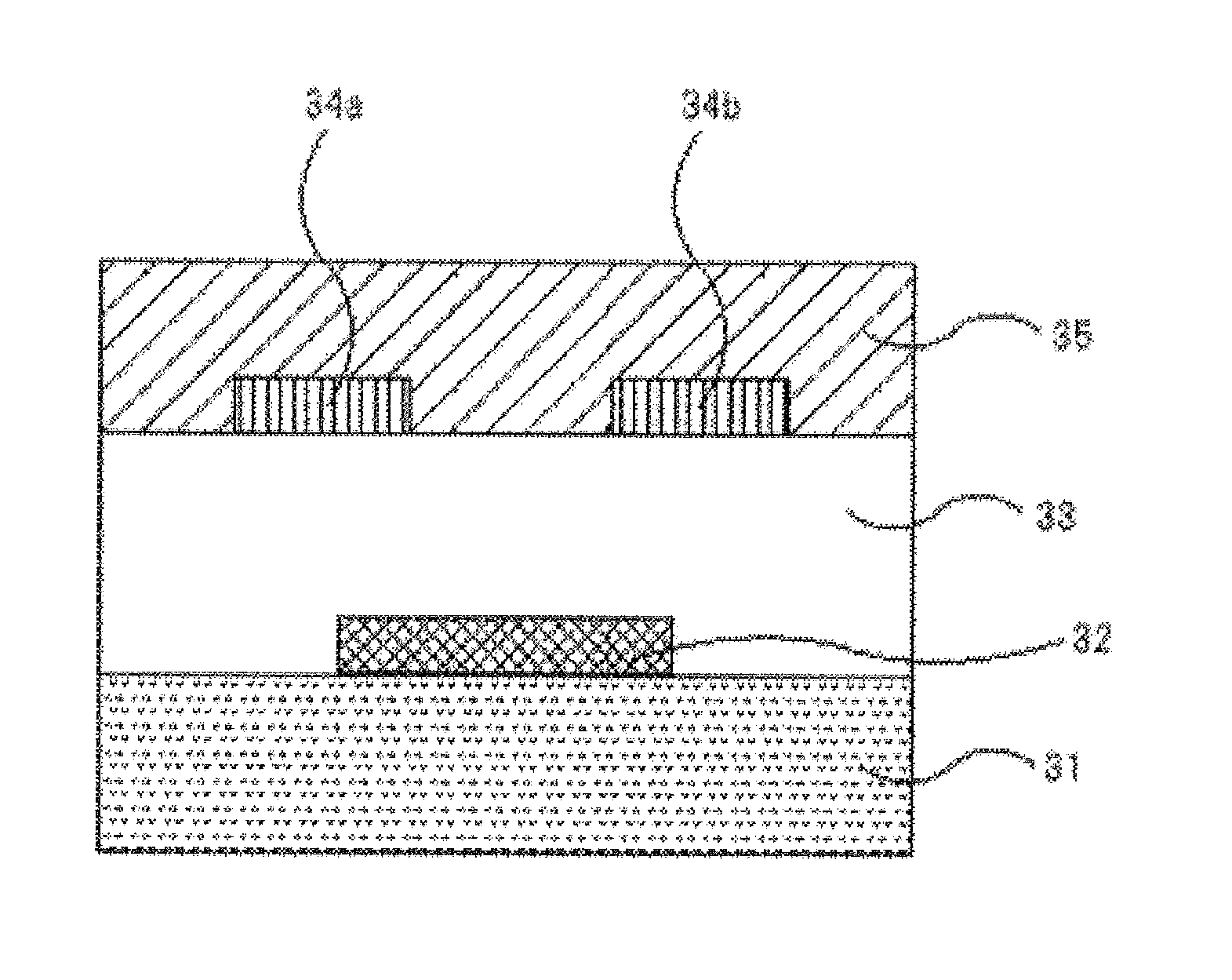
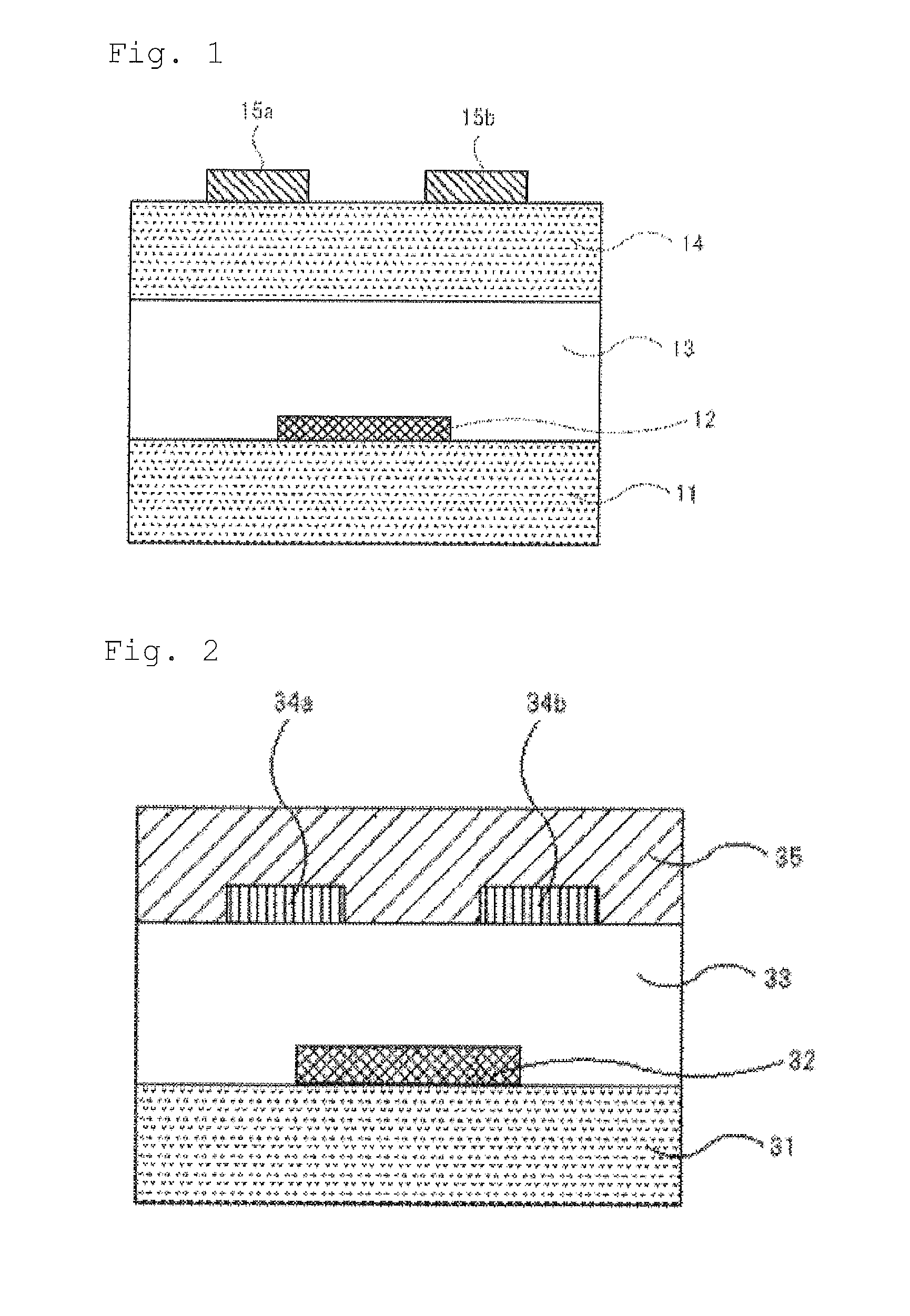
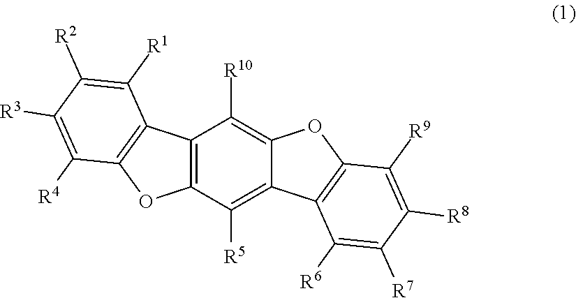
[0151]The compound represented by the general formula (1) or a comparative compound (1 mg) and 1,2-dichlorobenzene (1 mL) were mixed and heated to 100° C. The resulting solution was cast on an FET characteristics measuring substrate heated to 100° C. under a nitrogen atmosphere to provide an FET characteristics measuring device. The FET characteristics measuring substrate used was one shown in FIG. 2, which was a silicon substrate having a bottom-gate bottom-contact structure having source and drain electrodes formed of chromium-gold disposed in an interdigitated layout (gate width W=100 mm, gate length L=100 μm) and an insulator film formed of SiO2 (thickness: 200 nm). The FET characteristics were evaluated for the carrier mobility, the change in the mobility after storing under a high temperature and high humidity condition, and the change in the threshold voltage after repeated operation, unde...


PUM


Abstract

An organic thin film transistor having a semiconductor active layer containing a compound represented by the formula (1) has a high carrier mobility and a small change in the threshold voltage after repeated operation. R1 to R10 represent H or a substituent, provided that at least one of R1 to R4 and R6 to R9 represents a substituent represented by -L-R, L represents a specific divalent linking group, and R represents an alkyl group, an oligooxyethylene group, an oligosiloxane group, or a trialkylsilyl group.

Description

CROSS-REFERENCE TO RELATED APPLICATIONS[0001]This application is a Continuation of PCT International Application No. PCT / JP2013 / 071322, filed Aug. 7, 2013, which claims priority under 35 U.S.C. Section 119(a) to Japanese Patent Application No. 2012-187058 filed on Aug. 27, 2012 and Japanese Patent Application No. 2013-019584 filed on Feb. 4, 2013. Each of the above applications is hereby expressly incorporated by reference, in its entirety, into the present application.BACKGROUND OF THE INVENTION[0002]1. Field of the Invention[0003]The present invention relates to an organic thin film transistor, an organic semiconductor thin film, and an organic semiconductor material. Specifically, the invention relates to an organic semiconductor material for a non-light-emitting organic semiconductor device containing a compound having a benzobisbenzofuran (which may be hereinafter referred to as BBBF) structure, an organic semiconductor thin film containing the material, and an organic thin fil...

Claims


Application Information

Patent Timeline
IPC IPC(8): C07D493/04C07F7/08H01L51/00H01L51/05
CPCC07D493/04H01L51/0545C07F7/0852H01L51/0558H01L51/0065H01L51/0062C07F7/0812C07F7/0838H10K85/6574H10K10/466H01L2031/0344H01L2924/13069H10K85/649H10K85/653H10K10/484
Inventor KITAMURA, TETSUTAKAKU, KOJISOTOYAMA, WATARUHIRAI, YUKIKINOSHITA, MASARUSHIGENOI, YUUTA
Owner FUJIFILM CORP
Why Eureka
Try Eureka