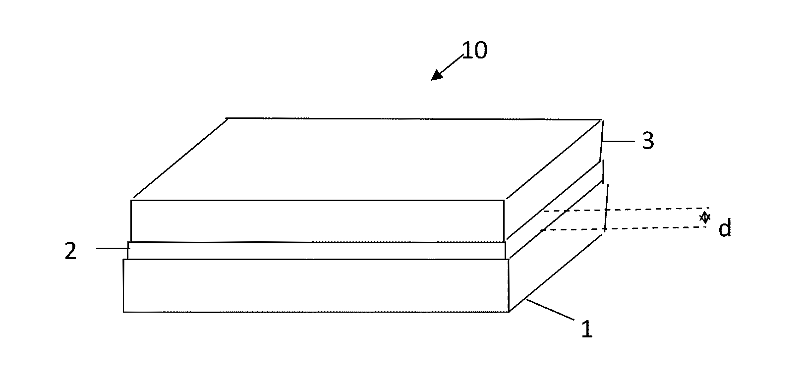
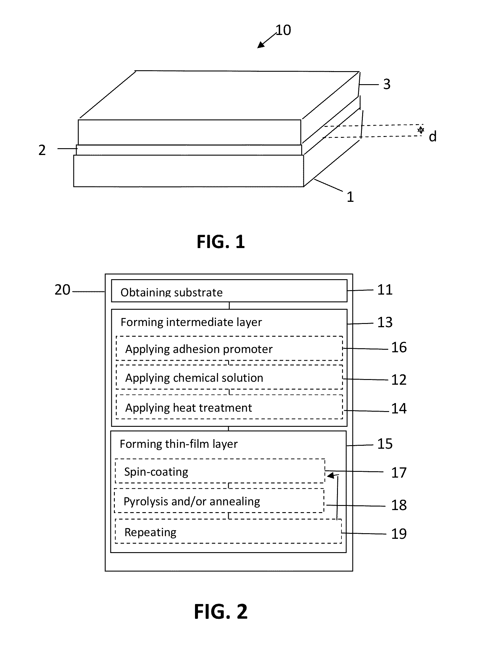
Preferentially oriented perovskite-related thin film
- Summary
- Abstract
- Description
- Claims
- Application Information
AI Technical Summary
Benefits of technology
Problems solved by technology
Method used
Image

Examples
first example
Preferentially Oriented BaTiO3 Thin Films Deposited on Silicon
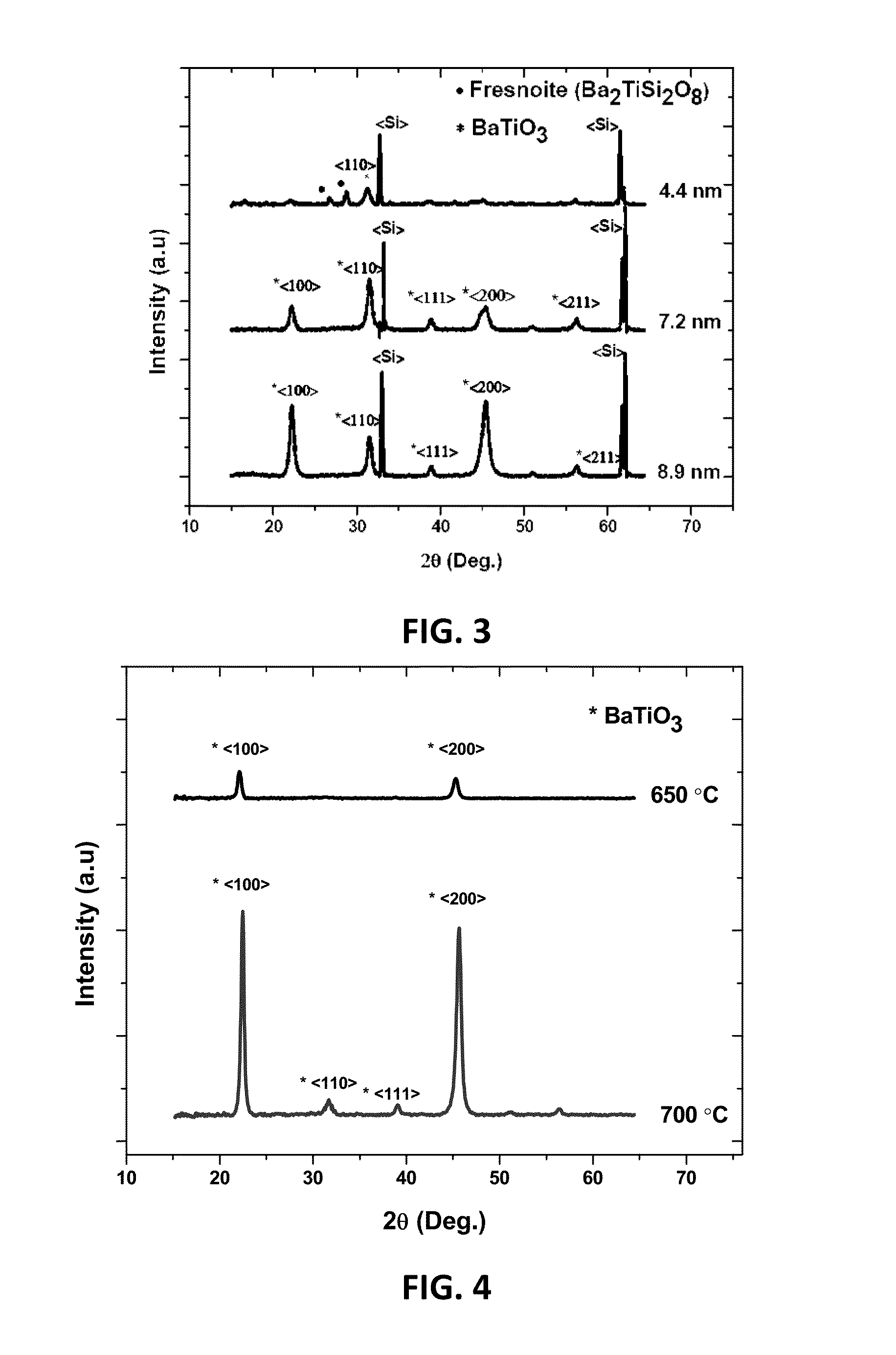
[0104]In this first example, Barium Titanate (BaTiO3) thin films are prepared with a conventional 2-methoxy ethanol based chemical solution deposition technique. Highly C-axis textured BTO thin films grown on silicon substrates with an ultra-thin intermediate layer of about 6 nm are attained by a method according to embodiments of the present invention. The influence of the intermediate layers as small as about 3 to 9 nm on the crystallization of BaTiO3 films is illustrated in detail. The annealing temperature and buffer layer sintering conditions are furthermore evaluated in order to obtain good crystal growth. X-ray diffraction measurements show the growth of well oriented BTO thin films having a single perovskite phase with a tetragonal geometry. SEM and AFM results indicate the presence of smooth, crack free, uniform layers, with well packed crystal grains on the silicon surface. The dielectric and P-E hysteresis beha...
second example
Sol-Gel Deposited PZT Thin Films Deposited on Silicon
[0124]In this second example, Lead Zirconate Titanate (PZT) thin films are deposited on silicon substrate with the conventional 2-methoxy ethanol based chemical solution deposition route. Intermediate layers as small as 4 nm can promote the PZT thin film growth on bare silicon substrate. The annealing temperature and buffer layer sintering conditions may be tuned so as to have an oriented thin film growth. X-ray diffractograms show preferentially oriented PZT thin films along the crystallographic orientation, having single perovskite phase with either tetragonal or rhombohedra geometry. Intermediate layers as thin as 4 nm can promote a preferentially oriented PZT thin film growth, with a dielectric constant of about 300, remnant polarization 2Pr˜16 μC / cm2, and coercive field Ec˜80 kV / cm. SEM and AFM measurements furthermore indicate the presence of smooth, crack free, uniform layers, with well packed PZT crystal grains of sizes ...
third example
Sol-Gel Deposited LiNbO3 Thin Films Deposited on Silicon
[0142]Lithium Niobate (LiNbO3) ceramic and thin film material has been used extensively for integrated optical applications, over the last few decades. Many electro-optic, piezo-electric and pyro-electric devices have been demonstrated already on this platform. High speed electro-optic optic modulators (40 Gbps) based on LiNbO3 are commercially available. In this example, it is demonstrated that highly c-axis textured lithium niobate films can be deposited on silicon platform with ultra thin intermediate layer (˜10 nm). The 2-methoxy ethanol sol-gel route similar to the two previous examples has been used to deposit LiNbO3 thin film on a silicon substrate.
[0143]Reagent grade Lithium ethoxide Li(CH3COO)2, and Niobium(V)Pentaethoxide Nb(C4H9O)4, were chosen as the source materials for lithium and niobium, whereas glacial acetic acid and 2-methoxy ethanol was used as the solvents. Firstly, lithium ethoxide is dissolved completely ...
PUM
| Property | Measurement | Unit |
|---|---|---|
| Temperature | aaaaa | aaaaa |
| Temperature | aaaaa | aaaaa |
| Thickness | aaaaa | aaaaa |
Abstract
Description
Claims
Application Information
 - Generate Ideas
- Intellectual Property
- Life Sciences
- Materials
- Tech Scout
- Unparalleled Data Quality
- Higher Quality Content
- 60% Fewer Hallucinations
Browse by: Latest US Patents, China's latest patents, Technical Efficacy Thesaurus, Application Domain, Technology Topic, Popular Technical Reports.
© 2025 PatSnap. All rights reserved.Legal|Privacy policy|Modern Slavery Act Transparency Statement|Sitemap|About US| Contact US: help@patsnap.com