

Negative electrode for lithium-ion secondary cell and method for manufacturing same
- Summary
- Abstract
- Description
- Claims
- Application Information
AI Technical Summary
Benefits of technology
Problems solved by technology
Method used
Image

Examples
example 1
[0104]A stainless steel sheet (SUS304 used in Example 1-1, SUS316 used in Example 1-2, and SUS430 used in Example 1-3) having a thickness of 1 mm was punched out to form a disc having a diameter of 16 mm, and this disc was used as the substrate.
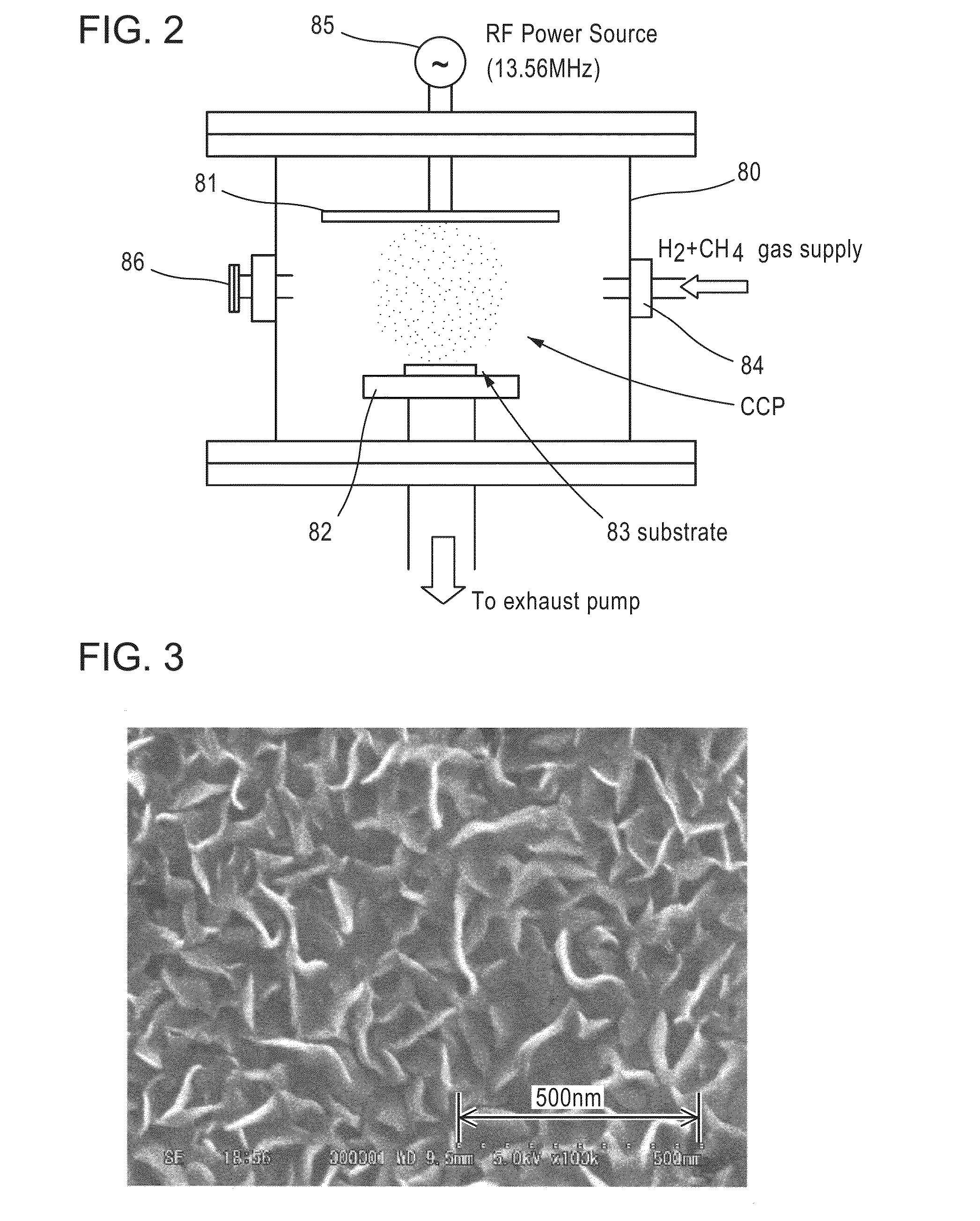
[0105]Next, after the stainless steel sheet punched out into a disc shape was placed in a chamber of a plasma CVD apparatus (see FIG. 2), plasma CVD was performed under the following conditions.
[0106]Flow gas mixed gas of hydrogen (10 percent by volume)+methane (50 percent by volume); Mixed gas flow rate 60 sccm; Substrate temperature 750° C.; Process pressure 0.1 torr (13.3 Pa); Time 1 hour; DC bias voltage 0 V; Output of applied high frequency wave 100W; Frequency of applied high frequency wave 13.56 MHz; Distance from electrode to substrate 25 mm.
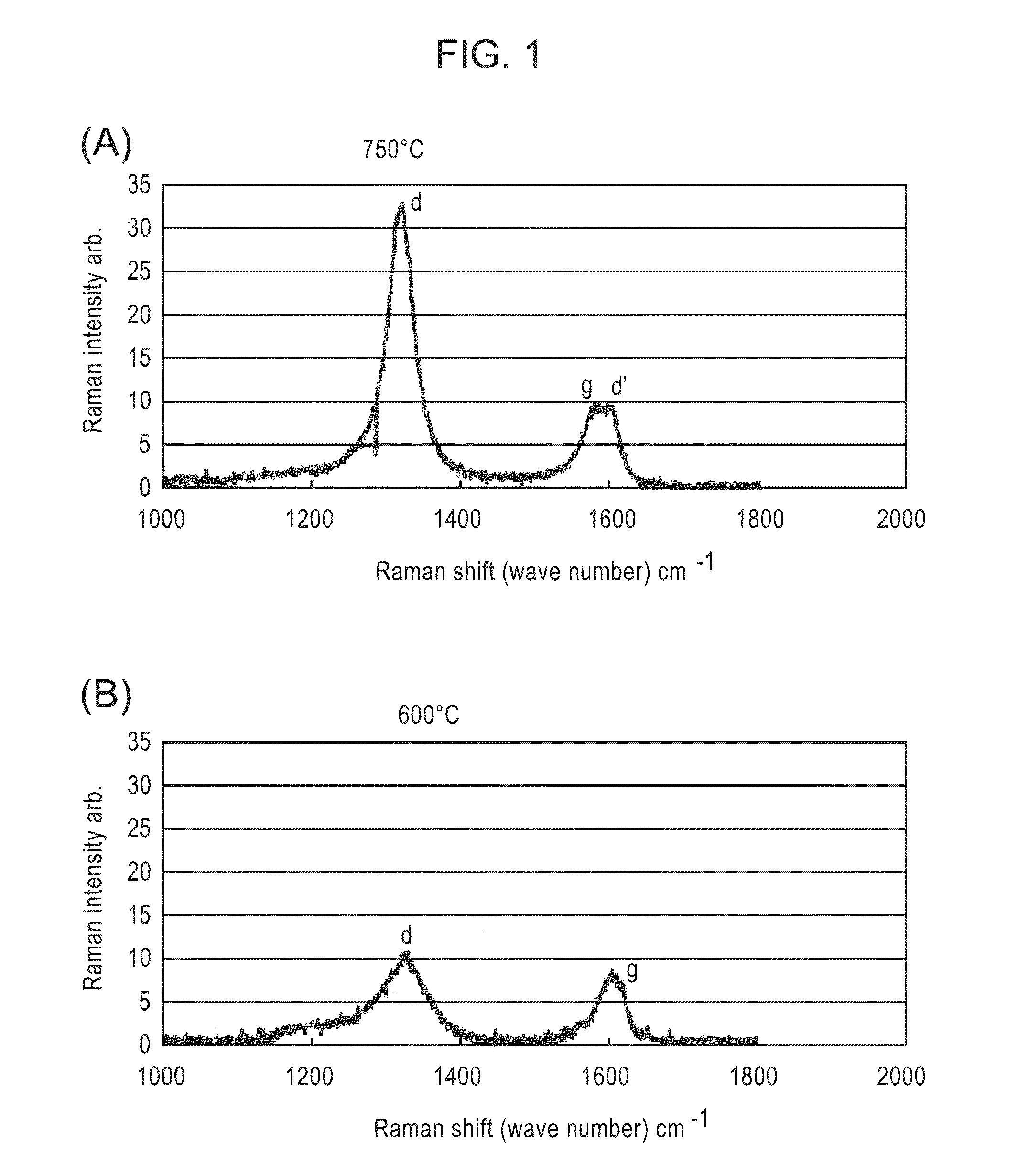
[0107]A scanning electron microscopic photo of a surface of a sample of Example 1-1 thus obtained is shown in FIG. 3. In addition, from transmission electron microscopic photos (see FIGS. 4 and 5)...
example 2
[0112]In Example 2, before the formation of the carbon nanochips layer by a plasma CVD in Example 1, in the state in which the substrate and the plasma CVD electrodes were set in the chamber, an oxygen cleaning step was performed under the following conditions. The other conditions were the same as those of Example 1 in which the formation of the carbon nanochips layer was performed by a plasma CVD method at a substrate temperature of 750° C., and description thereof will be omitted.
[0113]Flow gas 100% of oxygen; Gas flow rate 60 sccm; Substrate temperature controlled at 80° C. as minimum and 180° C. as maximum; Process pressure 0.8 Torr (100 Pa); Time 1 hour; Output of applied high frequency wave 100 W; Frequency of applied high frequency wave 13.56 MHz.
[0114]By the use of the negative electrode for a lithium-ion secondary cell formed as described above in each of Examples 1 and 2, a secondary cell (half cell) was formed using the carbon nanochips layer as a negative electrode surf...
example 3
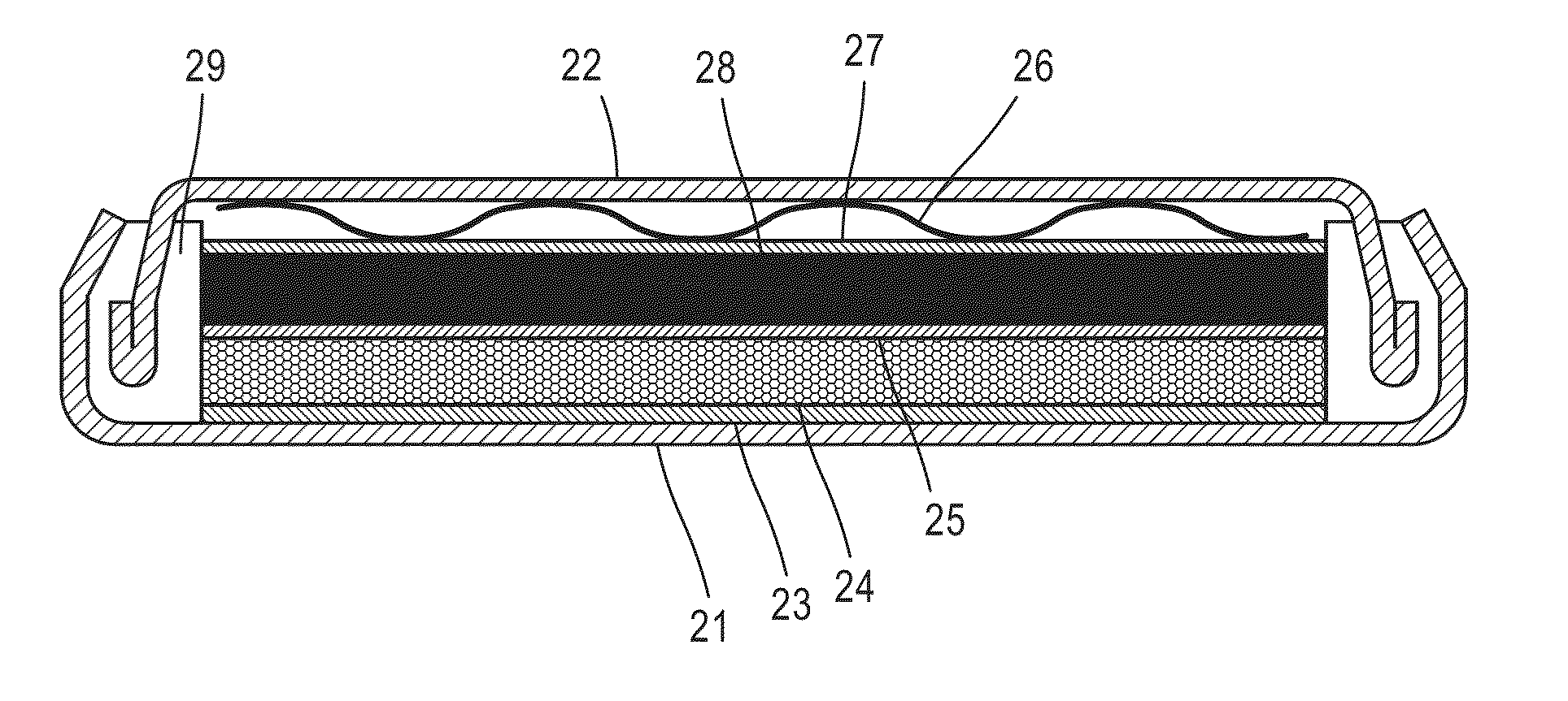
[0118]By the use of the negative electrode of Example 1, a full cell (coin cell: No. 2032) was formed, and the charge-discharge capacity thereof was measured. That is, as shown in FIG. 14, a positive electrode 28 containing a positive electrode active material Li1-xCoO2 (x=0 to 1, layered structure, capacity: 1.6 mAh / cm2) was brought into contact with a negative electrode 24 of Example 1 formed as described with a separator 25 provided therebetween, and a collector 27 using aluminum as a substrate was further brought into contact with the positive electrode 28 and was also brought into contact with a cell container 22 with a plate spring 26 provided therebetween. In addition, the negative electrode 24 was brought into contact with a cell container 21 with a collector 23 provided therebetween. In addition, as the electrolytic solution for a lithium-ion cell, a solution formed by dissolving LiPF6 in a mixed liquid containing ethylene carbonate and dimethyl carbonate at a mass ratio of...
PUM
 Abstract
Description
Claims
Application Information