Methods of low temperature deposition of ceramic thin films

a thin film, low temperature technology, applied in the direction of vacuum evaporation coating, boron compound, silicon compound, etc., can solve the problems of high defect density, design and operation of dual injector cvd reactor, and poor performance of the cvd reactor. , to achieve the effect of high commercial and technological value, the selection of substrates for the thin film is rather limited

Inactive Publication Date: 2015-11-19
GADGIL PRASAD NARHAR
View PDF9 Cites 15 Cited by
  • Summary
  • Abstract
  • Description
  • Claims
  • Application Information

AI Technical Summary

Benefits of technology

[0014]A method for low temperature deposition of ceramic thin film coatings of carbides, nitrides and mixed phases, the method includes determining deposition chemistries that employ combinations of reactive precursors to affect a required temperature for the deposition of the thin films to a surface of a substrate; loading the substrate into a process chamber; adjusting one or more process parameters including substrate temperature, chamber pressure, and chamber temperature; initiating a deposition cycle; determining whether a predetermined thickness of the thin film coating has been reached, and repeating the deposition cycles until the predetermined thickness has been reached; wherein the deposition is via atomic layer deposition (ALD), nano-layer deposition (NLD), or chemical vapor deposition (CVD); and wherein the combinations of reactive precursors are selected on the basis of reactivity between each of the reactive precursors as determined by the variation of Gibb's free energy (ΔG) with respect to deposition temperature in the chamber.
[0015]The method includes deposition of thin films of boron (B) carbides, nitrogen (N), nitrides, carbo-nitrides of silicon (Si), carbon (C), germanium (Ge), phosphorus (P), arsenic (As), oxygen (O), sulfur (S), and selenium (S). A higher negative value of Gibb's free energy of reaction forms the basis for selection of the reactive precursor combinations.

Problems solved by technology

Such requirements make design and operation of a dual injector CVD reactor rather complex.
Silicon nucleation is known to be highly detrimental to the SiC film quality in terms of defect density.
As a result of the required high process temperature, selection of substrates for these thin films, though of high commercial and technological value, is rather limited to ceramics, silicon, and quartz.
Furthermore, higher process temperatures invariably lead to a number of serious operational disadvantages that often limit commercial applications.
In terms of the final product, high operational temperatures lead to high in-film stress, extremely high defect density that severely degrades device performance.
Furthermore, inter-diffusion of layers, substrate warping, difficulties in integration with other thin films and impurity inclusion are serious issues of high process temperature.
In terms of equipment operation, issues of high power consumption, limits of selection of material of construction of the process chamber and its durability, gas flow stability, chemical precursor consumption and effluent treatment add to the cost and complexity.

Method used


Image

  • Methods of low temperature deposition of ceramic thin films
  • Methods of low temperature deposition of ceramic thin films
  • Methods of low temperature deposition of ceramic thin films

Examples


example 1

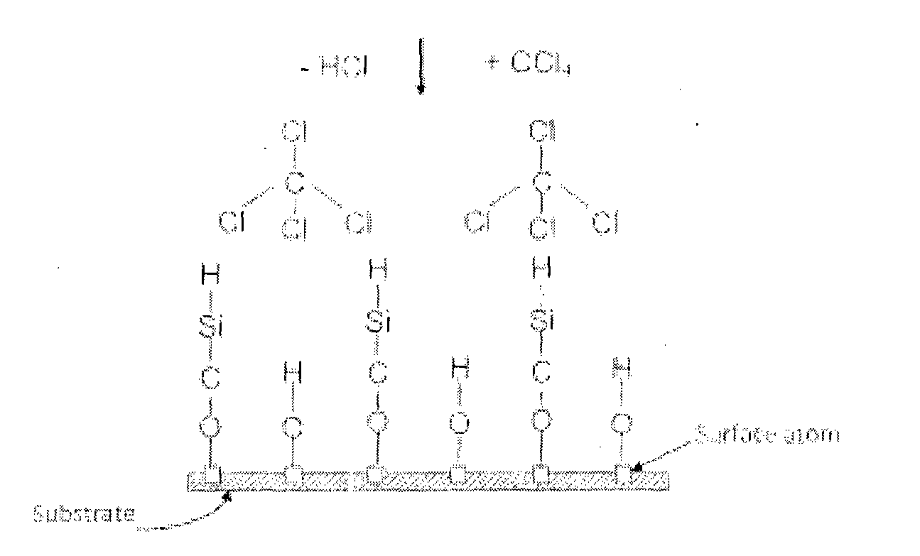
[0048]Deposition of silicon carbide (SiC) films by ALD, NLD and CVD processes: As described in the background section of the invention, SiC is an important industrial ceramic with numerous applications. However, the prevalent thin film deposition processes for SiC operates at temperatures in excess of 1000° C. Therefore, a low temperature ALD and also CVD SiC thin film process is thus highly desirable. Referring to FIG. 5A, the surface of a substrate is terminated with —OH groups which are highly receptive and reactive towards Cl atoms. Next in FIG. 5B wherein chemisorption of a carbon tetrachloride (CCl4) molecule (similar to a TiCl4 molecule as described in FIG. 1B) on to the —OH terminated substrate surface with the formation of HCl as a product that is released in the gas phase is completed. The substrate, at the end of CCl4 chemisorption step, is terminated with Cl groups with formation of a M-0-CCl3 (M: surface atom of the substrate, denoted by a square in FIGS. 5A, B, C and D...

example 2

[0051]Another thin film material of industrial value is boron nitride (BN). Thin films of BN are currently being deposited employing BCl3 and ammonia (NH3) at high temperature ranging from 700-1000° C. and above. FIG. 6B illustrates variation of Gibb's Free Energy (ΔG) vs. temperature for the following chemical reaction:

B2H6+2NF3→2BN+6HF  eq. (2)

[0052]The Very high value of ΔG vs. temperature of the reaction in equation (2) in comparison with the conventional BN process (ALD or CVD) illustrates the high value for developing a low temperature BN thin deposition process. The BN deposition process can be performed at pressures ranging from a few mT to 760 Torr and in the temperature range of 20° C. to 1000° C.

example 3

[0053]Deposition of C3N4 thin films: Processes of deposition and various applications of C3N4 as a thin film material have not yet been fully explored. It is expected to be one of the super-hard materials known. The formation of C3N4 films by ALD, NLD or CVD processes proceeds through carbon halide (e.g. CF4, CF2Cl2, or CCl4) as a carbon source, and NH3 as a nitrogen source in the temperature range of 20° C. to 1000° C., and in a pressure range of a few mT to 760 Torr. The overall chemical reaction of deposition (with CCl4 as a C source) is as follows:

3CF4+4NH3→C3N4+12HF  eq. (3)


PUM

PropertyMeasurementUnit
deposition ratesaaaaaaaaaa
temperaturesaaaaaaaaaa

Abstract

A method is provided for low temperature deposition of ceramic thin films of carbides, nitrides and mixed phases such as carbo-nitrides by atomic layer deposition (ALD), nano-layer deposition (NLD), and chemical vapor deposition (CVD). The deposition chemistries employ combinations of precursors to affect thin film processes at substantially lower temperatures than current deposition processes of thin films of boron (B) carbides, nitrogen (N), nitrides, carbonitrides of silicon (Si), carbon (C), germanium (Ge), phosphorus (P), arsenic (As), oxygen (O), sulfur (S), and selenium (S) on substrates. The inventive ALD and corresponding NLD and CVD process methods provide lower temperature deposition of various thin films comprising elements from the group B, C, Si, Ge, N, P, As and O, S and Se. The reactive precursor combinations are selected on the basis of reactivity towards one another as determined by the variation of Gibb's free energy (ΔG) with respect to deposition temperature.

Description

CROSS-REFERENCE TO RELATED APPLICATION[0001]This application claims priority of U.S. Provisional Patent Application Ser. No. 61 / 745,523 filed Dec. 21, 2012, which is incorporated herein by reference.FIELD OF THE INVENTION[0002]The present invention in general relates to the deposition of thin films, and in particular to methods of low temperature deposition of ceramic thin films of carbides, nitrides and mixed phases such as carbo-nitrides by atomic layer deposition (ALD), nano-layer deposition (NLD), and chemical vapor deposition (CVD).BACKGROUND OF THE INVENTION[0003]Thin films of carbides, nitrides and carbo-nitrides of silicon, germanium and boron and their mixed phases have significant and wide ranging applications in high temperature and high power electronic devices, sensors operating in harsh environments, corrosion and wear resistant coatings, and light emitting diode (LED) fabrication, etc. Prevalent methods of deposition of thin films of these materials include sputtering...

Claims


Application Information

Patent Timeline
Patent Type & Authority Applications(United States)
IPC IPC(8): C23C16/455C23C16/52
CPCC23C16/45553C23C16/45514C23C16/52H01L21/02529H01L21/02532H01L21/02573H01L21/0262C23C16/14C23C16/26C23C16/325C23C16/345H01L21/02112H01L21/02115H01L21/02167H01L21/0217H01L21/0228
Inventor GADGIL, PRASAD NARHARDUSZA, PETER JOSEPH
Owner GADGIL PRASAD NARHAR
Why Eureka
Try Eureka