
Apparatus and method for atomic force, near-field scanning optical microscopy

a near-field scanning and optical microscopy technology, applied in the field of high-resolution optical microscopy, can solve the problems of limiting the spatial resolution of an optical microscope, reducing the effective wavelength of reducing the speed of light with a high-refractive index material, so as to achieve the effect of limited spatial resolution improvement of immersion techniques, and limiting the spatial resolution of optical microscopes

Inactive Publication Date: 2015-11-26
MULTIPROBE
View PDF13 Cites 8 Cited by
  • Summary
  • Abstract
  • Description
  • Claims
  • Application Information

AI Technical Summary

Benefits of technology

This patent describes a special optical device that can bend light very tightly using a special waveguide. This device has a high refractive index and a specific shape that supports a certain type of light. The device also has a tapered section that helps to transform the light in a specific way. This transformation can be useful for a variety of applications. Overall, this device can provide better control over light bending and transformation, which can be useful for many different types of optical devices.

Problems solved by technology

[1] The diffraction of light ultimately limits the spatial resolution of an optical microscope that only couples propagating fields, to half of a wavelength.
[9] Since the optical frequency in a linear material remains the same, slowing down the speed of light with a high refractive index material reduces its effective wavelength.
The spatial resolution improvement of these immersion techniques is ultimately limited to the ratio of refractive indexes of the optic and object near-field.
[17] The significant improvement in spatial resolution with aperture NSOM designs is accompanied by a decrease in efficiency by many orders of magnitude, so it is not widely adopted outside of academia.
The decrease in efficiency from having a small area aperture in a large area optical field is commonly compounded by inefficient metallic waveguide designs placed before the aperture.
Polycrystalline metal coated fibers with conical tapers exhibit high power losses to heat in the coating, and only transmit through optical tunneling with modal cutoff before the aperture.
The heat absorption in the coating limits the input power that may be safely used before damage to the coating results.
However, the optical fiber used to fabricate standard NSOM probes has a relatively low refractive index, and therefore provide little benefit in spatial confinement.
Therefore coupling across the conical taper face introduces a large background (reflected or unconfined) signal, making spatial isolation and analysis difficult and the coupling efficiencies are poor, often below parts per million.
This type of thinking has led to limited development of a more effective NSOM design.
In addition to sacrifices in spatial confinement and therefore resolution, the fibers are also difficult to position and scan in the near-field.
As a requirement for NSOM however, methods for controlling the spacing as in scanned probe microscopy have been difficult to perform.
Neither of these techniques performs well as a scanned probe microscope.
However, since metals do not behave as perfect conductors at optical frequencies two effects result: First the actual antenna length for resonance is shorter than a quarter wavelength.
Second, since losses scale with interaction length, strong focusing of light to the smallest diffraction limited spot is necessary to maintain maximum efficiency, that is most of the squeezing of light should be done prior to coupling to the antenna.
High gain optical antennas are thus impractical in most applications due to losses from conduction resistance.
[21-30] As previously mentioned, aperture NSOM is impractical in most applications, because of its very low coupling efficiency.
Decreasing the angular semi-aperture or size of the near-field facet of a SIL significantly reduces both its spatial confinement and coupling efficiency, so it is only practical in applications where most of the angular semi-aperture is available.
Shaping the spherical surface of the SIL is also challenging from a fabrication cost perspective, and tends to drive its size up to the millimeter scale.
A hybrid NSOM design with a SIL and an antenna was proposed to create diffraction limited spatial confinement before reaching the antenna, but this design was never demonstrated and only overcomes one of the previously mentioned limitations associated with a SIL.
[32] Another hybrid NSOM design with an aperture and an antenna fabricated on an AFM cantilever demonstrated significantly higher efficiency than comparable aperture NSOM, but significantly lower efficiency than standard antenna NSOM, due to losses in the waveguide, aperture, and antenna composed of polycrystalline aluminum.
[29-30] A hybrid NSOM design called a Campanile with a partially coated waveguide and an antenna at the end of a glass optical fiber demonstrated spatial resolution improvement in one lateral direction but did not achieve maximum efficiency due to losses in the waveguide coating and antenna composed of polycrystalline gold.

Method used


Image

  • Apparatus and method for atomic force, near-field scanning optical microscopy
  • Apparatus and method for atomic force, near-field scanning optical microscopy
  • Apparatus and method for atomic force, near-field scanning optical microscopy

Examples


Embodiment Construction

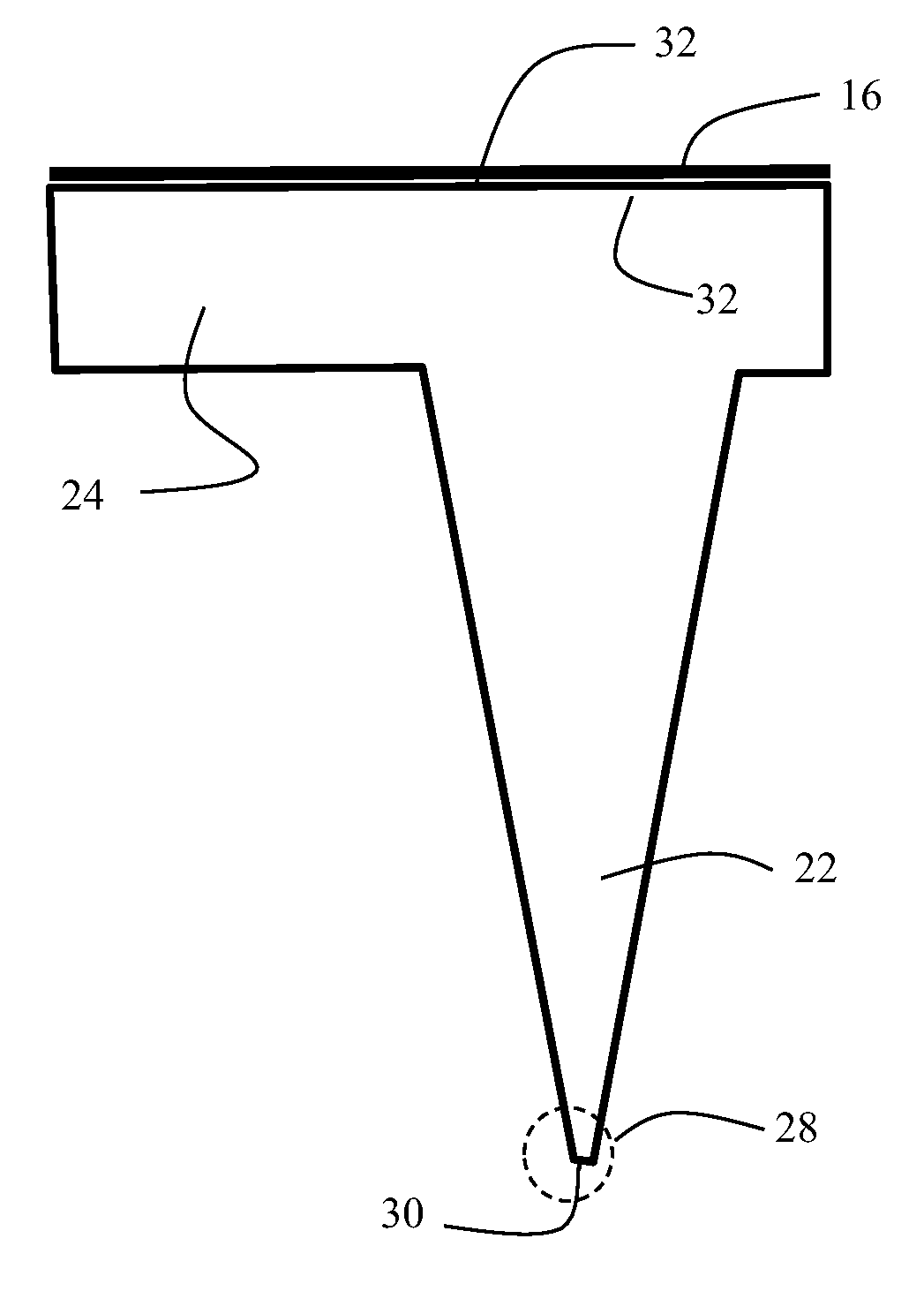
[0066]The embodiments described herein provide a first element where light is converted from free space propagation to near-field confinement. The near-field optic converts the free space beam with a diameter of several wavelengths to a diffraction limited spot size while simultaneously providing small semi-aperture and ease of manipulation. A high refractive index semiconductor waveguide with a tapered section disposed at the end of a cantilever accomplishes this spatial confinement up the ultimate diffraction limit with minimal angular semi-aperture and near unity efficiency.

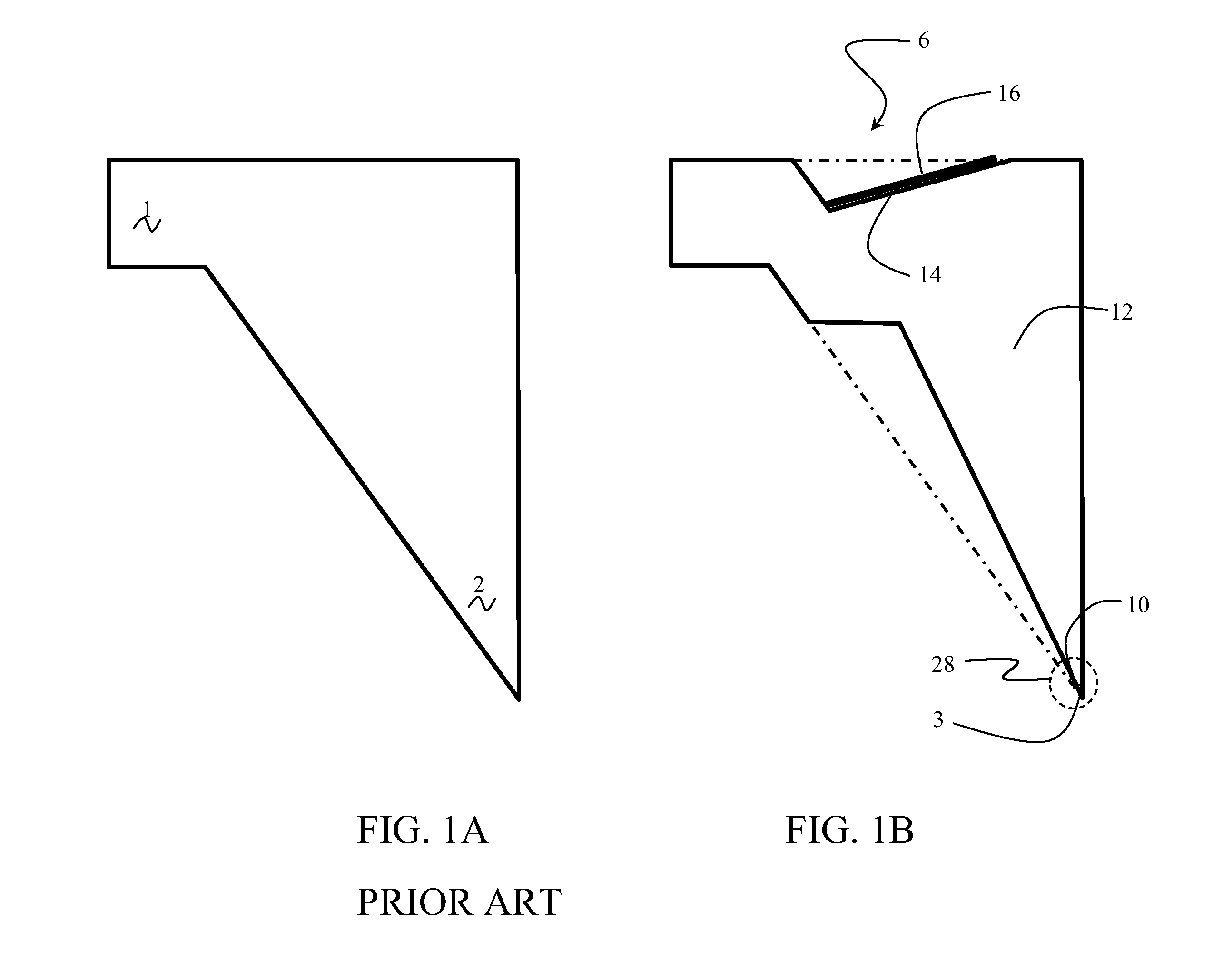
[0067]Referring to the drawings, FIG. 1A shows a standard tetrahedral silicon AFM probe, with a cantilever 1 and a tip 2. This standard silicon AFM probe design is not intrinsically useful for optical microscopy because the top surface is not orthogonal to the tetrahedral axis thereby leading to total internal reflection instead of external refraction. It also strongly couples light from the tip 2 into the can...


PUM

PropertyMeasurementUnit
refractive indexaaaaaaaaaa
thicknessaaaaaaaaaa
refractive indexaaaaaaaaaa

Abstract

A near-field optic has a high refractive index waveguide with a planar far field facet more than half of a wavelength across for coupling propagating light and a near field facet with the near field zone of the waveguide supporting only the fundamental optical mode in each polarization. A tapered waveguide section extends from the near field facet to transform the fundamental optical mode. A cantilever supports the tapered waveguide section.

Description

REFERENCES TO RELATED APPLICATIONS[0001]This application claims priority of U.S. Provisional Application Ser. No. 62 / 001,823 entitled Scanning Optical Microscopy filed on May 22, 2014, the disclosure of which is incorporated herein by reference.BACKGROUND INFORMATION[0002]1. Field[0003]Embodiments of the disclosure relate generally to the field of high resolution optical microscopy more particularly a near field optic incorporating a high refractive index semiconductor waveguide with a tapered section disposed at the end of a cantilever to provide spatial confinement up the ultimate diffraction limit with minimal angular semi-aperture and near unity efficiency with optional addition of an optical antenna at the tip of the waveguide employing a bisected gold nanorod forming a dipole optical antenna and gap.[0004]1. Background[0005]For a few centuries, optical microscopists have steadily improved the spatial resolution and efficiency of coupling light between small-scale objects and l...

Claims


Application Information

Patent Timeline
Patent Type & Authority Applications(United States)
IPC IPC(8): G02B21/00G02B6/26
CPCG02B21/0032Y10T409/303752G02B6/262G01Q60/06G01Q60/22G02B2006/12195G02B6/122
Inventor ERICKSON, ANDREW NORMANIPPOLITO, STEPHEN BRADLEYRILEY, ANTON LEWIS
Owner MULTIPROBE
Learn More