

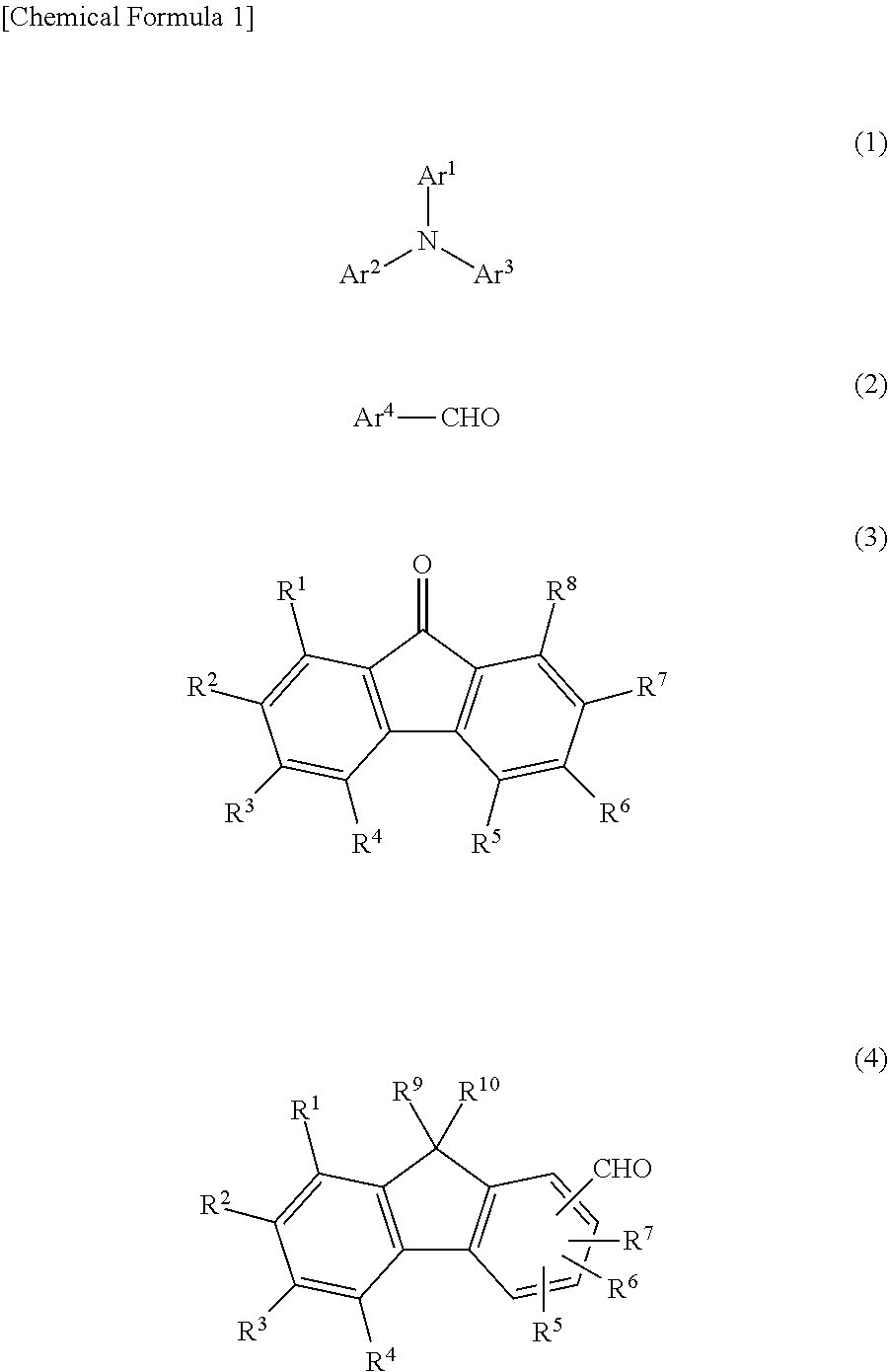
Charge-transporting varnish
a technology of charge-transporting varnish and charge-transporting spherical layer, which is applied in the direction of non-metal conductors, conductors, thermoelectric devices, etc., can solve the problems of requiring independent steps and the production process of organic el devices, and achieve excellent brightness characteristics and durability, and reduce costs
- Summary
- Abstract
- Description
- Claims
- Application Information
AI Technical Summary
Benefits of technology
Problems solved by technology
Method used
Image

Examples
synthesis example 1
Synthesis of Polymer 1
[0139]
[0140]The solution obtained by adding 10.0 g (40.76 mmol) of triphenylamine, 0.44 g (2.44 mmol) of pentafluorobenzaldehyde, 7.68 g (42.80 mmol) of 9-fluorenone and 1.62 g (8.15 mmol) of p-toluenesulfonic acid to 20 g of 1,4-dioxane was raised to a temperature of 110° C. and stirred in this state for 4 hours, then cooled to room temperature. After cooling, the solution was diluted by adding 10 g of tetrahydrofuran (THF), the diluted solution was added dropwise to 500 mL methanol / 100 mL 28% ammonia water, and the resulting mixture was stirred for 30 minutes. The powder that precipitated out was recovered by suction filtration and dissolved in 40 mL of THF. This solution was added dropwise to 500 mL of methanol and stirred for 30 minutes. The precipitated powder was recovered by suction filtration and vacuum dried, giving Polymer 1 (3.8 g).[0141]Mw (GPC): 1,800[0142]IR (cm−1): 1587, 1505, 1323, 1274, 1178, 1111, 1074, 993, 965, 750, 694, 632
synthesis example 2
Synthesis of Polymer 2
[0143]
[0144]The solution obtained by adding 10.0 g (40.76 mmol) of triphenylamine, 0.78 g (4.48 mmol) of pentafluorobenzaldehyde, 7.27 g (40.35 mmol) of 9-fluorenone and 1.62 g (8.15 mmol) of p-toluenesulfonic acid to 20 g of 1,4-dioxane was raised to a temperature of 110° C. and stirred in this state for 3 hours, then cooled to room temperature. After cooling, the solution was diluted by adding 10 g of tetrahydrofuran (THF), the diluted solution was added dropwise to 500 mL methanol / 100 mL 28% ammonia water, and the resulting mixture was stirred for 30 minutes. The powder that precipitated out was recovered by suction filtration and dissolved in 40 mL of THF. This solution was added dropwise to 500 mL of methanol and stirred for 30 minutes. The precipitated powder was recovered by suction filtration and vacuum dried, giving Polymer 2 (4.5 g).[0145]Mw (GPC): 1,900[0146]IR (cm−1): 1587, 1504, 1488, 1324, 1272, 1162, 1122, 1067, 1016, 819, 750, 692, 620
[2] Synthe...
synthesis example 3
Synthesis of Oligoaniline Compound 1
[0147]
[0148]Tetrakis(triphenylphosphine)palladium (0.5799 g, 0.5018 mmol) and 10.13 g (105.40 mmol) of sodium tert-butoxide were added to a mixed suspension of 10.00 g (50.19 mmol) of 4,4′-diaminodiphenylamine, 34.17 g (105.40 mmol) of 4-bromotriphenylamine and 100 g of xylene, and the mixture was stirred under nitrogen at 130° C. for 14 hours.
[0149]Next, the reaction mixture was filtered, saturated saline was added to the filtrate and liquid-liquid extraction was carried out, following which solvent was driven off by distillation from the organic phase. The solid thus obtained was recrystallized from 1,4-dioxane, giving the target Oligoaniline Compound 1 in an amount of 22.37 g (yield, 65%).
[0150]1H-NMR (CDCl3): δ 7.83 (S, 2H), 7.68 (S, 1H), 7.26-7.20 (m, 8H), 7.01-6.89 (m, 28H).
[3] Preparation of Charge-Transporting Varnish
PUM
| Property | Measurement | Unit |
|---|---|---|
| charge-transporting | aaaaa | aaaaa |
| electroluminescence | aaaaa | aaaaa |
| Charge-transporting | aaaaa | aaaaa |
Abstract
Description
Claims
Application Information