Composition for forming a coating type silicon-containing film, substrate, and patterning process

a technology of coating type and substrate, applied in the direction of coating, photomechanical equipment, instruments, etc., can solve problems such as damage to the substra

Active Publication Date: 2016-04-07
SHIN ETSU CHEM IND CO LTD
View PDF5 Cites 21 Cited by
  • Summary
  • Abstract
  • Description
  • Claims
  • Application Information

AI Technical Summary

Benefits of technology

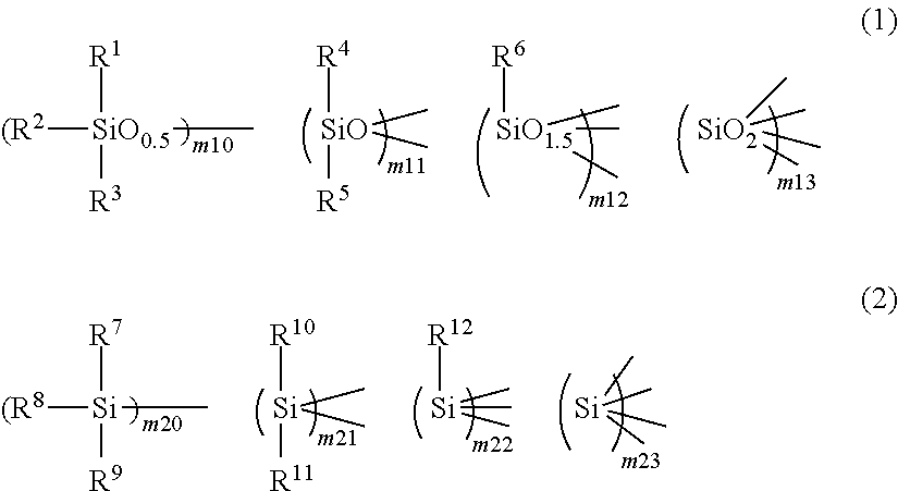
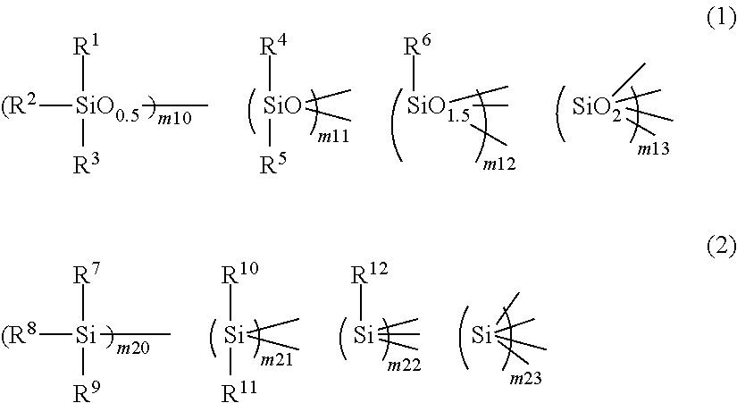
[0023]The present invention has been accomplished in view of the above-mentioned problem, and an object thereof is to provide a composition for forming a coating type silicon-containing film that has excellent adhesiveness in fine pattern, and can be easily wet etched by a removing liquid which does not cause damage to a semiconductor substrate and a coating type organic film or a CVD film mainly consisting of carbon which are necessary in the patterning process.
[0062]The coating type silicon-containing film formed by using the composition for forming a coating type silicon-containing film of the present invention may serve as a resist under layer film that has excellent adhesiveness to a photoresist pattern formed thereon and does not cause a pattern collapse even in a fine pattern. Moreover, this coating type silicon-containing film shows high etching selectivity to both of a resist pattern formed at the upper side and an organic film formed at the lower side, so that a formed photoresist pattern can be transferred to the substrate by dry etching process. Moreover, it can be easily wet etched by a removing liquid which does not cause damage to the semiconductor substrate and the coating type organic under layer film or the CVD film mainly consisting of carbon, and the silicon-containing film can be easily wet etched also in the retrying process.

Problems solved by technology

As mentioned above, when the conventional silicon-containing resist under layer film is used, problem arises that dry etching or a hydrofluoric acid type removing liquid causes damage to the substrate in the retrying process of patterning or in the manufacturing process of the semiconductor structure.

Method used


Image

  • Composition for forming a coating type silicon-containing film, substrate, and patterning process
  • Composition for forming a coating type silicon-containing film, substrate, and patterning process
  • Composition for forming a coating type silicon-containing film, substrate, and patterning process

Examples


examples

[0205]Hereinafter, the present invention will be specifically described with reference to Preparation Examples, Synthesis Examples, Examples, and Comparative Examples, but the present invention is not restricted thereto. In the following examples, “%” represents “% by mass”, and molecular weight was measured by GPC. Molecular weight was calculated by GPC in terms of polystyrene, using RI detector and tetrahydrofuran as an eluent.

Preparation of Polysilane Compound

Preparation Example (X1)

[0206]10.0 g of OGSOL SI-10-20 (Mw 1,900) available from Osaka Gas Chemicals Co., Ltd., was dissolved in 100.0 g of tetrahydrofuran, and then 6.0 g of triethylamine and 16.0 g of ultrapure water were added thereto. After the resulting solution was reacted for 7 hours under reflux, 375 g of propylene glycol monoethyl ether (PGEE) was added thereto, and the mixture was concentrated under reduced pressure to obtain 91.3 g of a PGEE solution containing polysilane compound (X1) (polymer concentration: 11%)...

preparation example (

X3)

[0208]10.0 g of OGSOL SI-20-10 (improved) (Mw 1,400) available from Osaka Gas Chemicals Co., Ltd., was dissolved in 100.0 g of tetrahydrofuran, and then 6.0 g of triethylamine and 16.0 g of ultrapure water were added thereto. After the resulting solution was reacted for 12 hours under reflux, 250 g of propylene glycol monoethyl ether (PGEE) was added thereto, and the mixture was concentrated under reduced pressure to obtain 71.3 g of a PGEE solution containing polysilane compound (X3) (polymer concentration: 14%) with a Mw of 830.

[0209]In the following, formulation amounts of Preparation Examples (X1) to (X3) are summarized in Table 1.

TABLE 1PreparationExamplesRaw materials for reactionMwX1SI-10-20: 10.0 g980X2SI-20-10: 10.0 g870X3SI-20-10 (improved): 10.0 g830

Synthesis Example (A1)

[0210]To a mixture comprising 120 g of PGEE, 1 g of 70% nitric acid, and 60 g of deionized water was added a mixture comprising 17.0 g of methyl trimethoxy silane (M1), 5.0 g of phenyl trimethoxy silan...

synthesis example (

C4)

[0220]To a mixture comprising 120 g of methanol, 1 g of methanesulfonic acid, and 60 g of deionized water was added a mixture comprising 34.1 g of methyl trimethoxy silane (M1) and 67.6 g of 4-tert-butoxyphenyl trimethoxy silane (M8), and the resulting mixture was maintained at 40° C. for 12 hours to carry out hydrolysis condensation. After completion of the reaction, 500 g of PGEE was added thereto, and a by-produced alcohol and excess water were distilled off under reduced pressure to obtain 570 g of a PGEE solution containing polymer (C4) (polymer concentration: 12%). The molecular weight of the obtained polymer was measured in terms of polystyrene, consequently finding a Mw of 2,700.

Synthesis Examples (C5) to (C11)

[0221]PGEE solutions containing polymers (C5) to (C11) were obtained in the same manner as in Synthesis Example (C4) by using monomers shown in Table 3.

[0222]In the following, formulation amounts of Synthesis Examples (C1) to (C11) are summarized in Table 3.

TABLE 3S...


PUM

PropertyMeasurementUnit
wavelengthaaaaaaaaaa
sizeaaaaaaaaaa
sizeaaaaaaaaaa

Abstract

A composition for forming a coating type silicon-containing film, containing one or more silicic acid skeletal structures represented by the formula (1) and one or more silicon skeletal structures represented by the formula (2), wherein the composition contains a coupling between units shown in the formula (2). There can be provided a composition capable of forming a silicon-containing film that has excellent adhesiveness in fine patterning, and can be easily wet etched by a removing liquid which does not cause damage to a semiconductor substrate and a coating type organic film or a CVD film mainly of carbon which is required in the patterning process.

Description

BACKGROUND OF THE INVENTION[0001]1. Field of the Invention[0002]The present invention relates to a composition for forming a coating type silicon-containing film usable in a process for producing a semiconductor device and so forth, a substrate having a film formed from the composition, and a patterning process using the composition.[0003]2. Description of the Related Art[0004]In 1980s, photo-exposure using g-beam (436 nm) or i-beam (365 nm) of mercury lamp as a light source had been widely used in the resist patterning. As a means for finer patterning, shifting to a exposure light having shorter wavelength was assumed to be effective, so that, for the mass production process of DRAM (Dynamic Random Access Memory) with 64 MB (work size of 0.25 μm or less) in 1990s and later ones, KrF excimer laser (248 nm), whose wavelength is shorter than i-beam (365 nm), had been used in place of i-beam as the exposure light source.[0005]However, for production of DRAM with integration of 256 MB a...

Claims


Application Information

Patent Timeline
Patent Type & Authority Applications(United States)
IPC IPC(8): C09D183/00G03F7/11H01L21/3213H01L21/308H01L21/311
CPCC09D183/00H01L21/3086G03F7/11H01L21/31144H01L21/32139H01L21/3081H01L21/02126H01L21/02211H01L21/02216H01L21/02282H01L21/0332H01L21/31111C09D183/10C08G77/48G03F7/0752
Inventor TACHIBANA, SEIICHIROTANEDA, YOSHINORIKIKUCHI, RIEOGIHARA, TSUTOMU
Owner SHIN ETSU CHEM IND CO LTD
Why Eureka
Try Eureka