Method of manufacturing semiconductor device

a manufacturing method and technology of semiconductor devices, applied in the direction of semiconductor devices, basic electric elements, electrical equipment, etc., can solve the problems of not being able to heat all of the transition metal layers simultaneously, the material configuring the device, etc., and the interface properties of the semiconductor portion and gate insulating film may degrade,

Active Publication Date: 2016-06-30
FUJI ELECTRIC CO LTD
View PDF7 Cites 6 Cited by
  • Summary
  • Abstract
  • Description
  • Claims
  • Application Information

AI Technical Summary

Benefits of technology

[0110]The method of manufacturing a semiconductor device according to the present invention achieves an effect in that an ohmic contact of low contact resistivity can be formed and device properties can be prevented from degrading.

Problems solved by technology

Nonetheless, in Japanese Laid-Open Patent Publication Nos. 2012-246216, 2009-177102, and 2011-066060, the portion forming the ohmic contact (i.e., the transition metal layer, or the interface of the substrate and the transition metal layer) cannot be selectively heated; rather the entire substrate (the entire device) is uniformly heated.
Therefore, interface properties of the semiconductor portion and gate insulating film, the material configuring the device, etc. may degrade.
Therefore, in cases where the distance from the converging lens to the surface of the transition metal layer is not constant consequent to the transition metal layer being disposed in a chip side wall or a trench side wall, throughput may decrease since laser irradiation has to be performed according to conditions corresponding to each irradiation position and therefore, not all of the transition metal layer can be simultaneously heated.
Further, with Japanese Laid-Open Patent Publication No. 2012-099599, since a predetermined region is selectively heated by laser irradiation, programming control for irradiation position, irradiation loci, etc. of the laser is complicated.
Furthermore, irradiation voids occur consequent to deviation of the laser irradiation position, whereby contact resistivity becomes inconsistent; and near the transition metal layer, constituent portions (e.g., gate insulating film, etc.) other than the transition metal layer are heated, whereby device properties may degrade.
Furthermore, if the surface area of the transition metal layer is smaller than the area corresponding to the spot diameter of the laser, a problem arises in that the transition metal layer cannot be selectively heated alone.
Therefore, a problem arises in that the hydrogen atom density becomes low and consequently rapid heating is not possible.
In practice, in Republished Japanese-Translation of PCT Application, Publication No. 2009-118783, since plasma processing at a low electrical power of 200 W to 500 W is performed for a long period, during the plasma processing, constituent portions other than the transition metal layer (e.g., the entire device) are heated by a transfer of the heat generated by the transition metal layer and as a result, device properties may degrade.

Method used


Image

  • Method of manufacturing semiconductor device
  • Method of manufacturing semiconductor device
  • Method of manufacturing semiconductor device

Examples


first embodiment

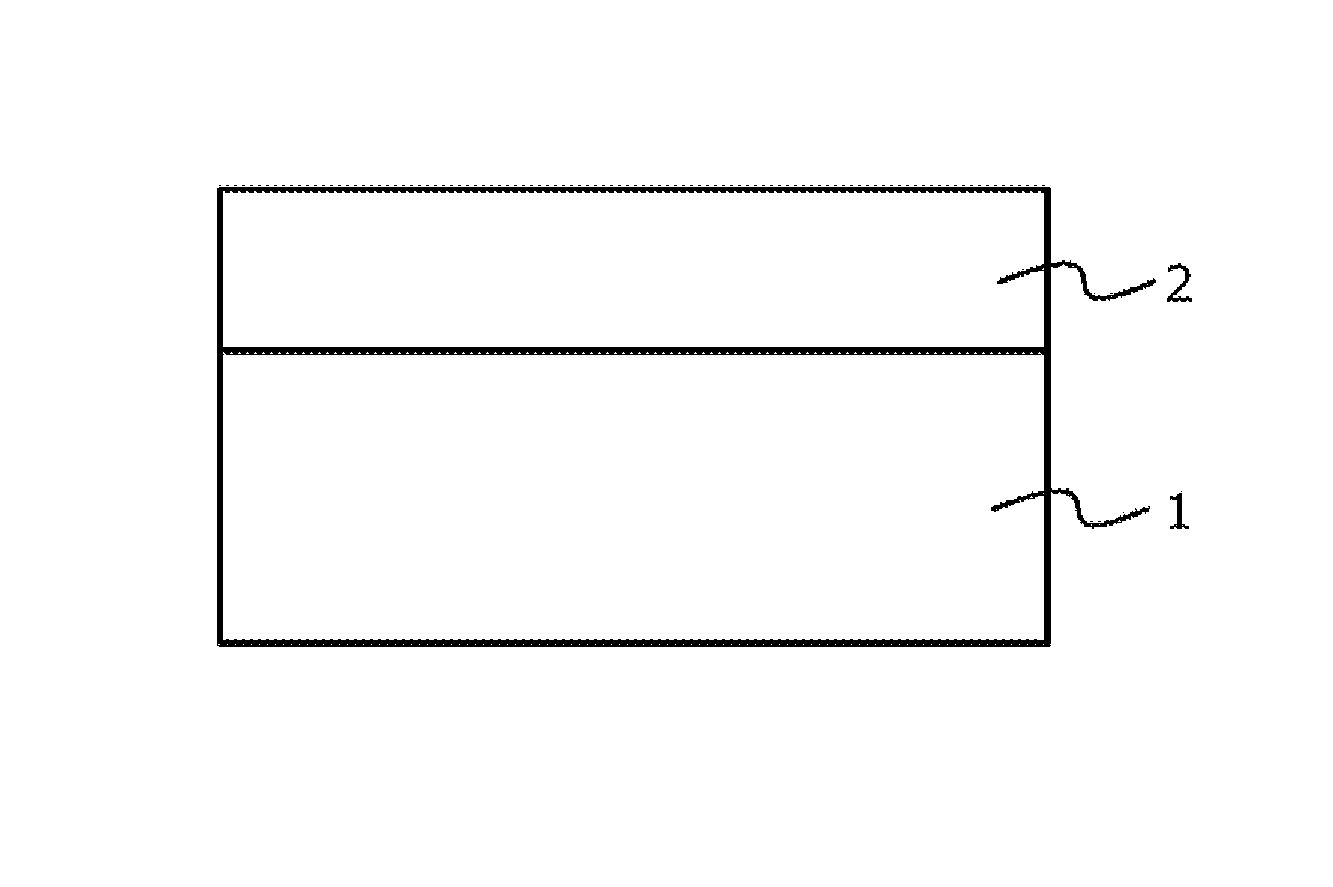
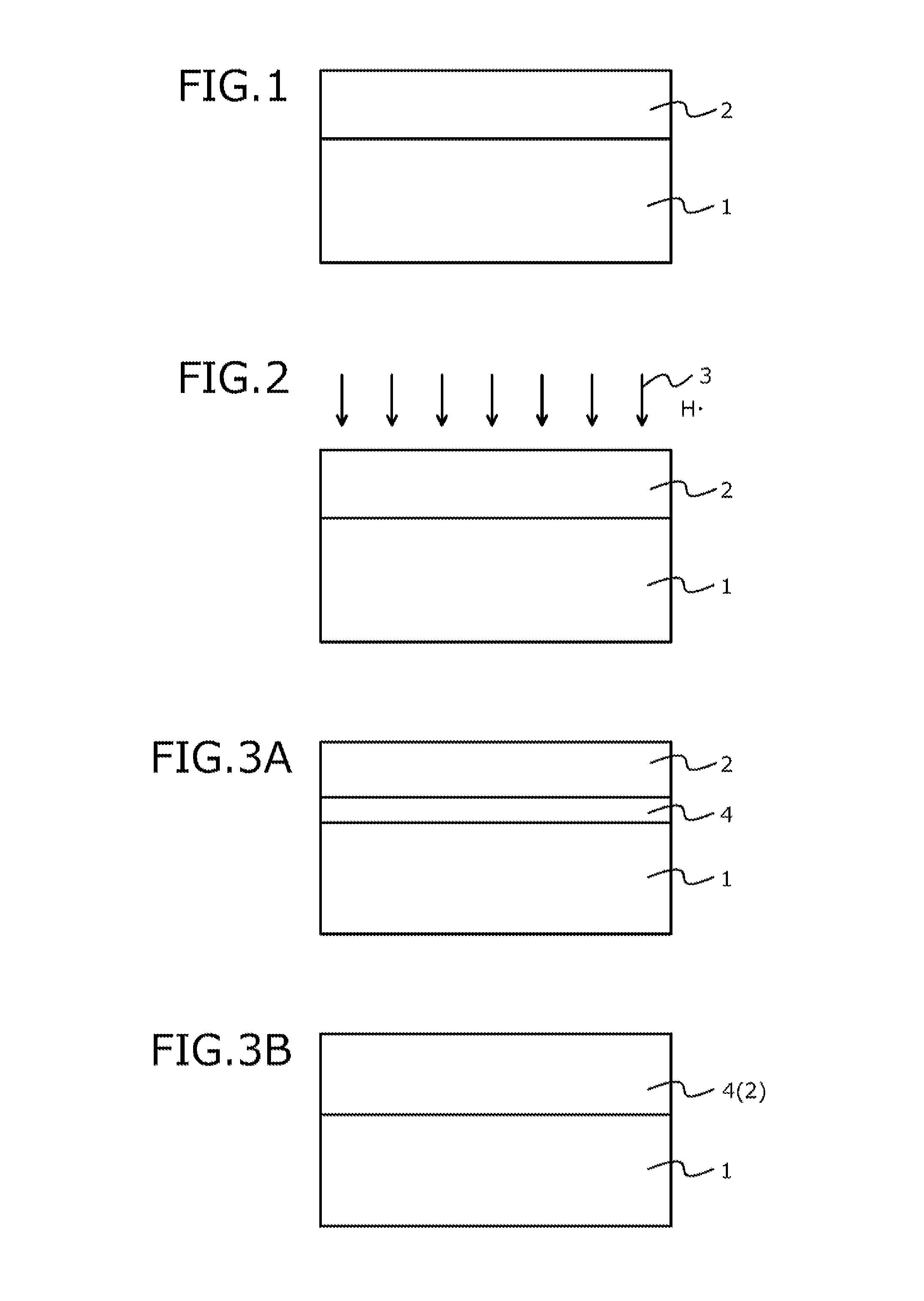
[0058]The method of manufacturing a semiconductor device according to a first embodiment will be described taking an example where a semiconductor device using a silicon carbide semiconductor substrate (silicon carbide substrate) is produced (manufactured). FIGS. 1, 2, and 3A are cross-sectional views of a semiconductor device during manufacture according to the first embodiment. FIG. 3B is a cross-sectional view of another example of a semiconductor device during manufacture according to the first embodiment. First, as depicted in FIG. 1, a predetermined device structure (not depicted) is formed in a silicon carbide substrate (silicon carbide wafer) 1 and subsequently a contact electrode 2 formed of a transition metal is formed in a surface of the silicon carbide substrate 1 by, for example, a sputtering method, a vapor deposition method, etc.

[0059]The transition metal configuring the contact electrode 2 is an element (metal) present within a range from the third element group to t...

second embodiment

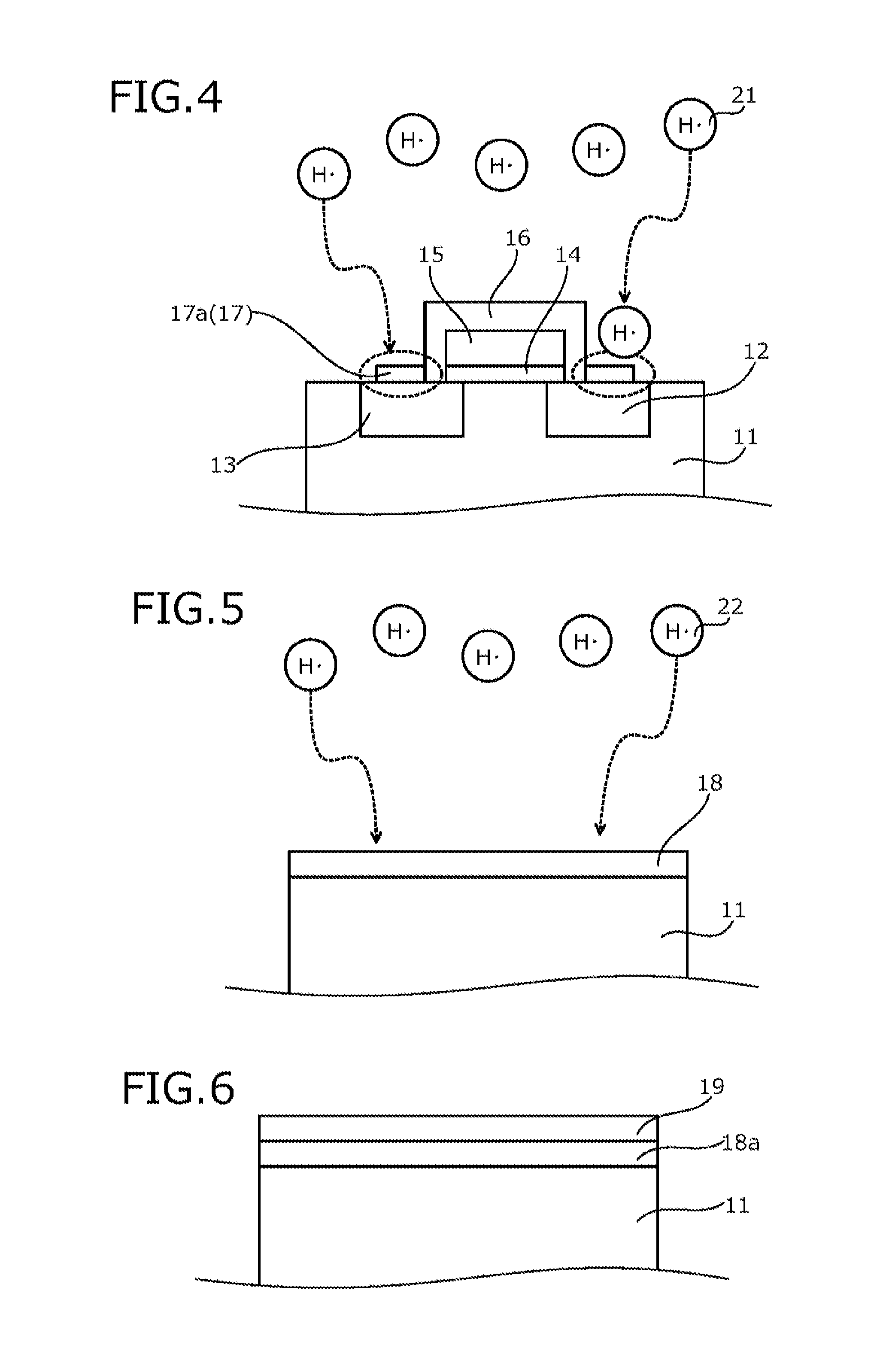
[0077]The method of manufacturing a semiconductor device according to a second embodiment will be described taking an example where an ohmic contact is formed in the back surface of a silicon carbide substrate. FIGS. 7, 8, and 9 are cross-sectional views of the substrate back surface side of a semiconductor device during manufacture according to the second embodiment. The method of manufacturing a semiconductor device according to the second embodiment differs from the method of manufacturing a semiconductor device according to the first embodiment in that after a titanium layer 23 is formed on a transition metal layer (e.g., the nickel layer 18) that is to be converted to silicide, the entire silicon carbide substrate (the entire device) is exposed to the hydrogen plasma atmosphere. The titanium layer 23 has a function of preventing the nickel silicide layer 18a formed by a reaction of the nickel layer 18 and a silicon carbide semiconductor portion (the drift region 11) from being ...

third embodiment

[0085]The method of manufacturing a semiconductor device according to a third embodiment will be described taking as an example, a case where a MOSFET is formed. FIG. 10 is a cross-sectional view of a semiconductor device during manufacture according to the third embodiment. The method of manufacturing a semiconductor device according to the third embodiment differs from the method of manufacturing a semiconductor device according to the first embodiment in that with the nickel layers 17, 18 formed on both surfaces of the silicon carbide substrate, a quartz substrate 24 is disposed so as to contact the entire surface of the nickel layer 18 of the substrate back surface side and the entire silicon carbide substrate (the entire device) is exposed to the hydrogen plasma atmosphere.

[0086]More specifically, as depicted in FIG. 10, similar to the first embodiment, processes up to and including those of forming the nickel layers 17, 18 in the surfaces of the silicon carbide substrate respe...


PUM

PropertyMeasurementUnit
thicknessaaaaaaaaaa
thicknessaaaaaaaaaa
thicknessaaaaaaaaaa

Abstract

A method of manufacturing a semiconductor device includes providing a semiconductor substrate having a front surface and a back surface; forming a transition metal layer in a surface of the semiconductor substrate; and exposing the semiconductor substrate having the transition metal layer formed thereon to a hydrogen plasma atmosphere formed by microwaves, to cause the transition metal layer to generate heat, Thus, during the exposure of the semiconductor substrate, a portion of the semiconductor substrate contacting the transition metal layer is heated by a transfer of heat from the transition metal layer and, at an interface of the transition metal layer and the semiconductor substrate, an ohmic contact is formed by reaction of the transition metal layer and the semiconductor substrate, such as to form a transition metal silicide when the semiconductor substrate is silicon carbide. The ohmic contact provides a lower contact resistivity and device properties can be prevented from degrading.

Description

CROSS REFERENCE TO RELATED APPLICATIONS[0001]This is non-provisional application is a continuation of International Application PCT / JP2015 / 061899 filed on Apr. 17, 2015, which claims priority from Japanese Patent Application No. 2014-086709 filed on Apr. 18, 2014, the contents of both of which are incorporated herein by reference.BACKGROUND OF THE INVENTION[0002]1. Field of the Invention[0003]The embodiments discussed herein are related to a method of manufacturing a semiconductor device.[0004]2. Description of the Related Art[0005]Conventionally, in a semiconductor device (semiconductor apparatus) that uses (Si) semiconductor, a silicon carbide (SiC) semiconductor, etc., an ohmic contact (electrical contact portion) of a semiconductor portion and a transition metal layer (electrode) is formed by heat treatment (annealing). Here, a method of forming an ohmic contact in a conventional semiconductor device will be described taking an example where a nickel (Ni) contact electrode is fo...

Claims


Application Information

Patent Timeline
Patent Type & Authority Applications(United States)
IPC IPC(8): H01L21/285H01L21/04
CPCH01L21/28518H01L21/28568H01L21/0485H01L21/049H01L21/043H01L21/28H01L29/1608H01L29/45H01L29/66068H01L29/665H01L29/78H01L2924/0002H01L2924/00
Inventor NAKAZAWA, HARUOOGINO, MASAAKINAKAJIMA, TSUNEHIROIGUCHI, KENICHITACHIOKA, MASAAKINAKAGAWA, KIYOKAZU
Owner FUJI ELECTRIC CO LTD
Why Eureka
Try Eureka