
Method for fabricating nanogap electrodes, nanogap electrodes array, and nanodevice with the same

a nano-gap electrode and array technology, applied in nanoinformatics, liquid/solution decomposition chemical coatings, coatings, etc., can solve the problems of microfabrication bringing significant technical problems, leakage current, and the possibility of fabricating a device difficult to achieve using, so as to reduce some distance, improve accuracy and yield ratio, the effect of high accuracy

Inactive Publication Date: 2016-10-13
JAPAN SCI & TECH CORP
View PDF3 Cites 0 Cited by
  • Summary
  • Abstract
  • Description
  • Claims
  • Application Information

AI Technical Summary

Benefits of technology

This approach enables the fabrication of nanogap electrodes with precise control over gap separation, improving the yield ratio and allowing for the creation of devices such as diode elements and single-electron devices with enhanced performance.

Problems solved by technology

On the other hand, the microfabrication brings about significant technical problems such as a short channel effect, velocity saturation, quantum effect, and so on.
This phenomenon is considered as one of possible cause of a leakage current due to the microfabrication of device.
Furthermore, in combination with the top-down method, the method for fabricating the nanogap electrodes and the nanogap electrodes fabricated using this method makes it possible to fabricate a device difficult to be achieved using the top-down method only, e.g., a transistor with a channel length of 5 nm or under.
All the previously reported methods used for fabricating nanogap electrodes have a problem: mechanical break junction method to break a thin line by a mechanical stress (Non-Patent Literature 5 and 6) allows an accurate picometer-order, however, it is not good for integration; electro-migration method is a comparatively easy one, (Non-Patent Literature 7 and 8), however, the yield ratio is low and fine metal particles between the nanogaps are often problematic for measurement when breaking a line; other methods having a good accuracy is not desirable for integration, still others require an extremely low temperature environment to prevent gold migration or need long processing time (Non-Patent Literature 9 to 14).

Method used


Image

  • Method for fabricating nanogap electrodes, nanogap electrodes array, and nanodevice with the same
  • Method for fabricating nanogap electrodes, nanogap electrodes array, and nanodevice with the same
  • Method for fabricating nanogap electrodes, nanogap electrodes array, and nanodevice with the same

Examples


example 1

[0142]As an example 1, nanogap electrodes are fabricated as follows using the molecular ruler electroless plating method, described in the first embodiment.

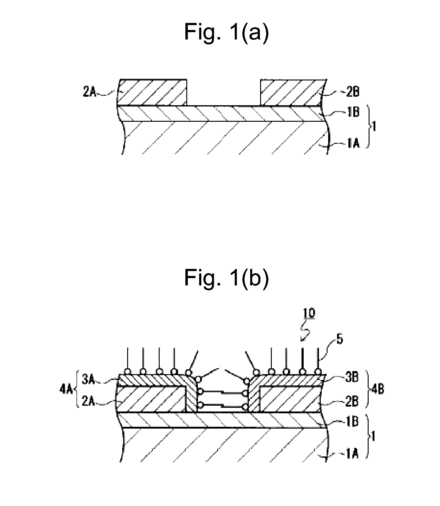
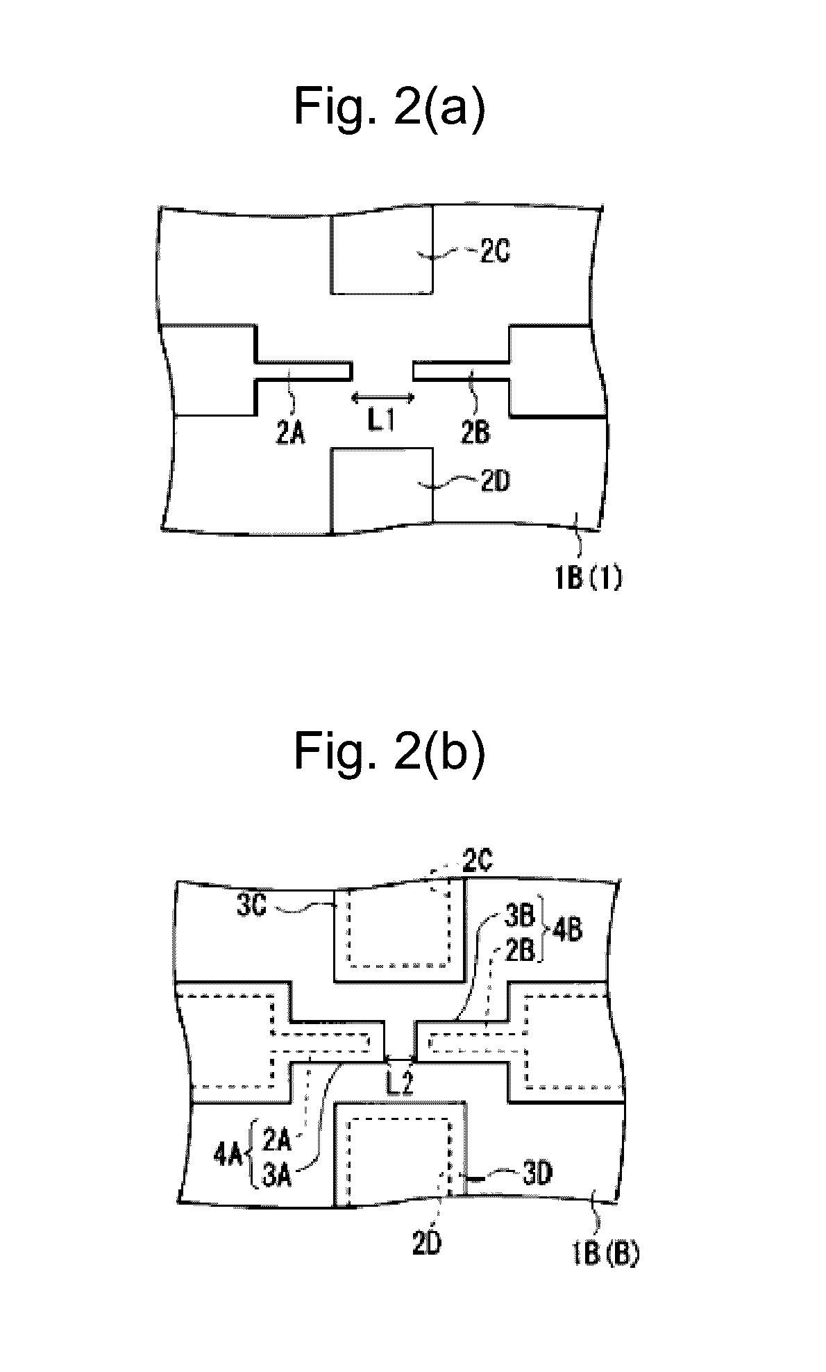
[0143]First, a silicon substrate (substrate 1A) on which a silicon dioxide film (insulating film 1B) is thoroughly provided is prepared. Then the substrate 1 is coated with resist and a pattern of initial electrodes (metal layers 2A, 2B with 30 nm gap separation) is drawn using the EB lithographic technology. After development, a 2 nm-Ti film is evaporated by EB evaporation and, on the Ti film, 10 nm Au is evaporated so that initial gold nanogap electrodes (metal layers 2A, 2B) is fabricated. A plurality of pairs of metal layers 2A, 2B are provided on the same substrate 1.

[0144]Next, an electroless plating solution is prepared. 28 mL (milliliter) of 25 mM (millimole) alkyltrimethylammonium bromide is measured to be used as a molecular ruler. Then, 120 μL it (microliter) of 50 mM chlorauric acid solution is measured and added ther...

example 2

[0154]In the example 2, nanogap electrodes are fabricated using the molecular ruler electroless plating method same as in the example 1 except for using LTAB molecule as alkyltrimethylammonium bromide.

[0155]FIG. 11 is an SEM image showing an example of the nanogap electrodes fabricated in the example 2. The gap separation in FIG. 11 (a) and (b) are respectively 1.98 nm and 2.98 nm.

example 3

[0156]In the example 3, nanogap electrodes are fabricated using the molecular ruler electroless plating method same as in the example 1 except for using MTAB molecule as alkyltrimethylammonium bromide. FIG. 12 is an SEM image showing an example of the nanogap electrodes fabricated in the example 3. The gap separation in FIG. 12 (a) and (b) are respectively 3.02 nm and 2.48 nm.


PUM

PropertyMeasurementUnit
channel lengthaaaaaaaaaa
lengthaaaaaaaaaa
molecular lengthaaaaaaaaaa

Abstract

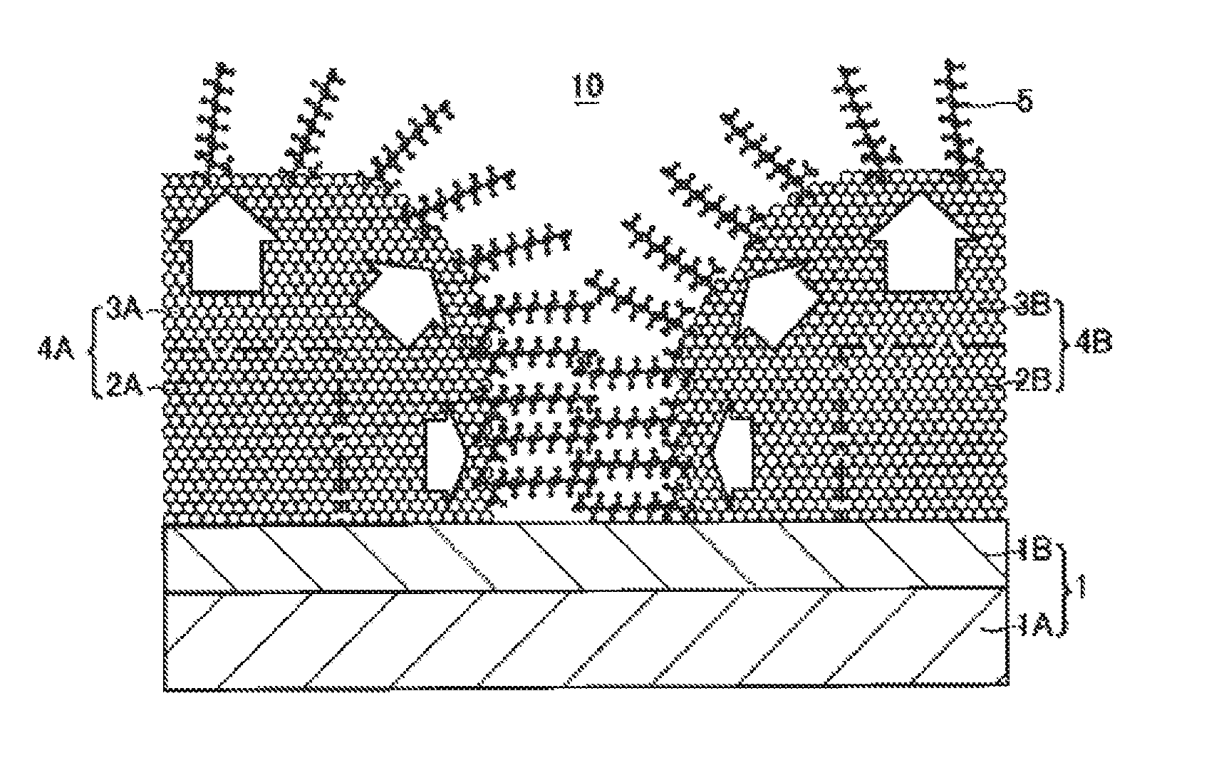
A substrate 1 having metal layers 2A and 2B arranged to form a gap is dipped in an electroless plating solution mixed an electrolyte solution including metal ions with a reducing agent and a surfactant. Metal ions are reduced by the reducing agent to be precipitated on the metal layers 2A and 2B, and the surfactant is adhered to a surface of the metal on the metal layers, thereby forming a pair of electrodes 4A, 4B to be controlled to have a nanometer sized gap. These steps enable to provide a method for fabricating nanogap electrodes, a nanogap electrodes array, and a nanodevice with the same.

Description

[0001]This application is a divisional of U.S. application Ser. No. 14 / 003,679, filed on Sep. 6, 2013, which is a National Stage of International Application No. PCT / JP2012 / 055002, filed on Feb. 28, 2012, which claims priority to Japanese priority application No. 2011-050894 filed on Mar. 8, 2011, which are hereby incorporated by reference.TECHNICAL FIELD[0002]The present invention relates to a method for fabricating nanogap electrodes, a nanogap electrodes array, and a nanodevice with the same.BACKGROUND ART[0003]It is a highly integrated VLSI system accompanying microfabrication of CMOS and a rapid growth in the field of semiconductor device such as DRAM and NAND flash memory that supports the advanced information society. Development of higher integration density, i.e., microfabrication of minimum processing size, has improved performance and functionality of electronic devices. On the other hand, the microfabrication brings about significant technical problems such as a short ch...

Claims


Application Information

Patent Timeline
Patent Type & Authority Applications(United States)
IPC IPC(8): H01L29/41H01L29/66H01L21/288H01L29/76
CPCH01L29/413H01L21/288H01L29/66439H01L29/7613B82Y10/00B82Y40/00H01L21/76838C23C18/1607C23C18/161C23C18/44H01L29/0673B82B1/00B82B3/00H01L21/18
Inventor MAJIMA, YUTAKATERANISHI, TOSHIHARUMURAKI, TAROTANAKA, DAISUKE
Owner JAPAN SCI & TECH CORP
Learn More