Oxide sintered body, method for producing same and sputtering target

a technology of sputtering target and oxidized body, which is applied in the direction of basic electric elements, electrical apparatus, metal material coating process, etc., can solve the problems of abnormal discharge or particle generation, and achieve the effects of reducing target resistance, and increasing the mobility of oxide semiconductors

Inactive Publication Date: 2016-11-24
IDEMITSU KOSAN CO LTD
View PDF3 Cites 8 Cited by
  • Summary
  • Abstract
  • Description
  • Claims
  • Application Information

AI Technical Summary

Benefits of technology

[0041]In the oxide sintered body of the invention, as other metal elements, Sn and / or Ge may be appropriately added. The amount added is normally 50 to 30000 ppm, preferably 50 to 10000 ppm, more preferably 100 to 6000 ppm, further preferably 100 to 2000 ppm, with 500 to 1500 ppm being particularly preferable. If Sn and / or Ge are / is added within the above-mentioned concentration range, In in the bixbyite phase is partially solid solution-substituted by Sn and / or Ge. As a result, electrons as a carrier generate, whereby resistance of the target can be decreased. Contents of other metal elements contained in the sintered body can also be obtained by quantitative analysis by Inductively Coupled Plasma Atomic Emission Analysis apparatus (ICP-AES) as in the case of In, A and B.
[0042]In order to increase the mobility of an oxide semiconductor obtained by using the oxide sintered body of the invention, it is preferable to add a positive tetravalent element such as Sn in a concentration of 50 to 30000 ppm.
[0043]In general, mobility of an oxide semiconductor is increased by increasing carrier concentration generated due to oxygen deficiency. However, this oxygen deficiency tends to change by bias stress or heat stress test, and as a result, a problem arises in operational reliability.
[0044]By addition of a positive tetravalent element according to the invention, oxygen deficiency can be sufficiently reduced by inclusion of the elements A and B that stably bond with oxygen, and carriers in a semiconductor channel can be controlled (channel doping). As a result, it is possible to attain high mobility and operational reliability.
[0045]In order to allow the effects of channel doping to be exhibited sufficiently, the content of a positive tetravalent element such as Sn is preferably 100 to 15000 ppm, further preferably 500 to 10000 ppm, and particularly preferably 1000 to 7000 ppm. If the content of a positive tetravalent element exceeds 30000 ppm, the carrier concentration may be increased excessively to cause a normally-on state. If the content of the positive tetravalent element is less than 50 ppm, while the resistance of the target is decreased, the effect of controlling the carrier concentration in the channel is not exhibited.
[0046]If the substrate with an oxide semiconductor film being formed thereon is quickly heated, e.g. is directly input in a furnace heated to 300° C., radially-shaped crystals tend to grow. Further, if the temperature is elevated slowly, i.e. 10° C. / min or lower, facet-shaped crystals tend to grow. The effect of channel doping depends on the crystallization temperature rather than the crystal form. Therefore, it is important to determine the crystallization temperature and crystallization time while confirming the effect of channel doping.

Problems solved by technology

However, by adding desirable elements in order to improve mobility or reliability of a TFT, the resistance of a target may be increased, resulting in occurrence of abnormal discharge or generation of particles.
However, a process of introducing water has problems that it requires sufficient removal in advance of oxygen or nitrogen that has been dissolved in water, as well as a new countermeasure such as prevention of corrosion of a piping has become necessary.

Method used


Image

  • Oxide sintered body, method for producing same and sputtering target
  • Oxide sintered body, method for producing same and sputtering target
  • Oxide sintered body, method for producing same and sputtering target

Examples


examples

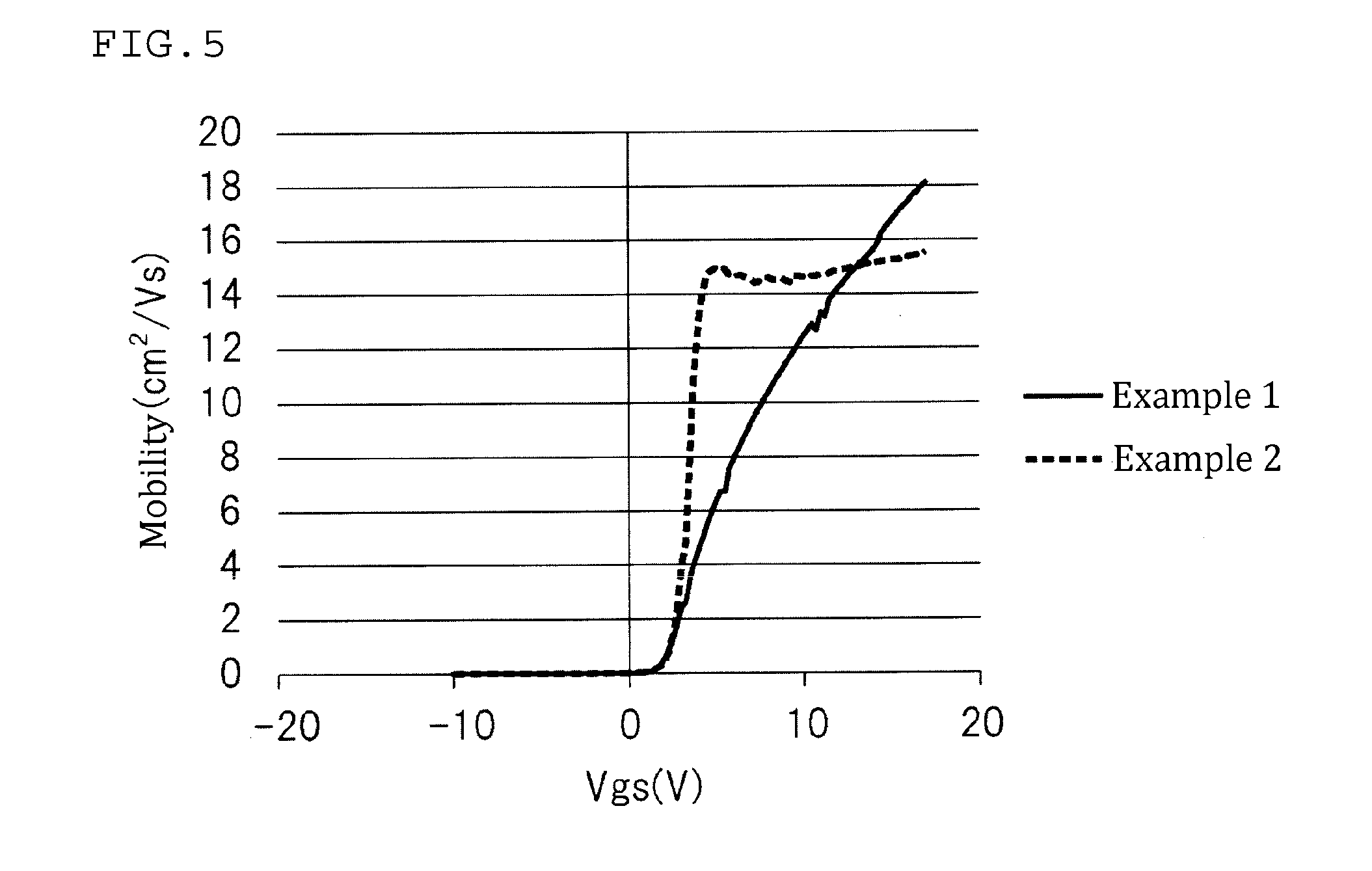
[0096]Hereinbelow, the invention will be explained in more detail with reference to the Examples which should not be construed as limiting the gist of the invention. The invention can be implemented by appropriately modifying within the scope of the invention, and such modifications fall within the scope of the invention.

examples 1 to 15

Production of Sintered Body

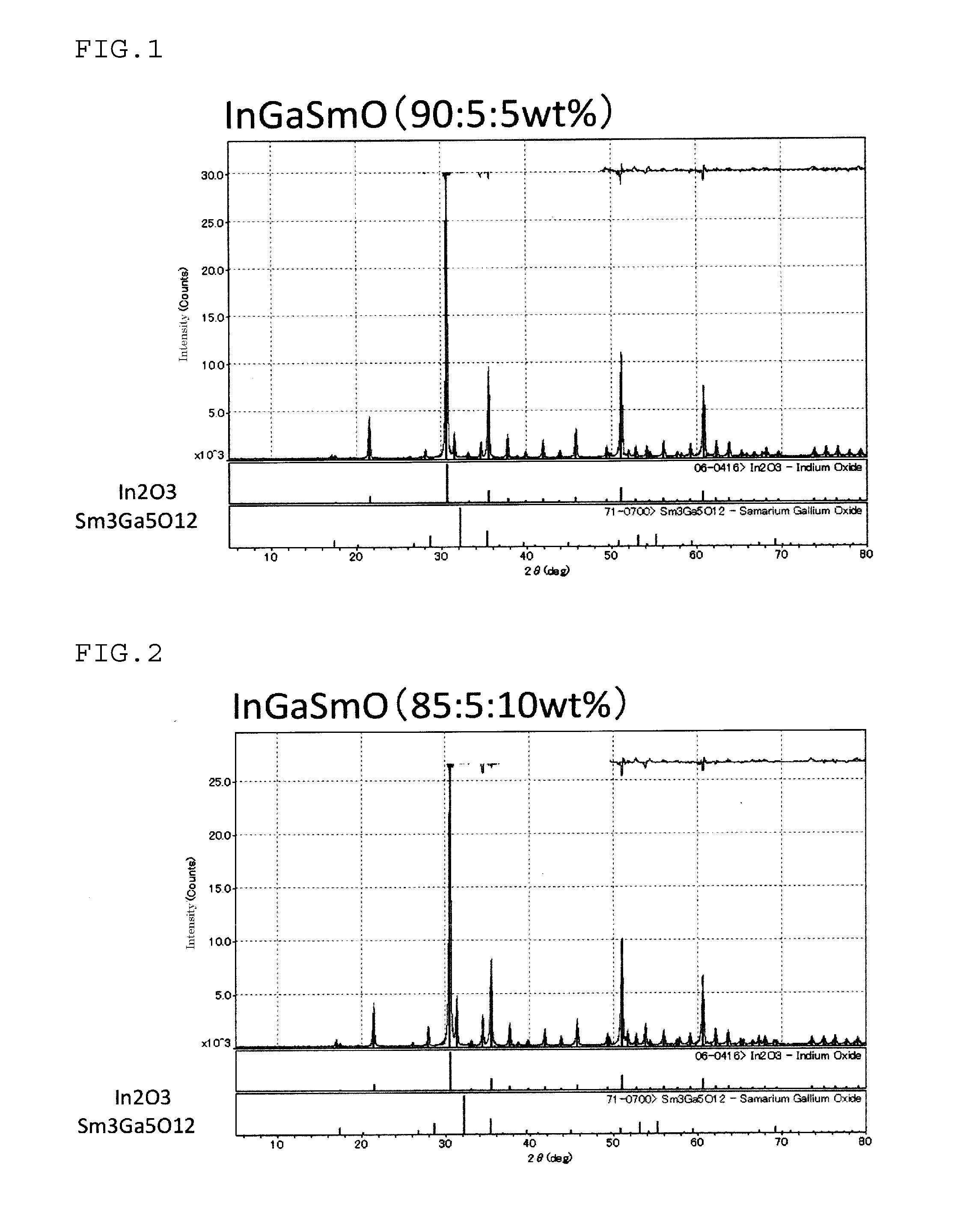
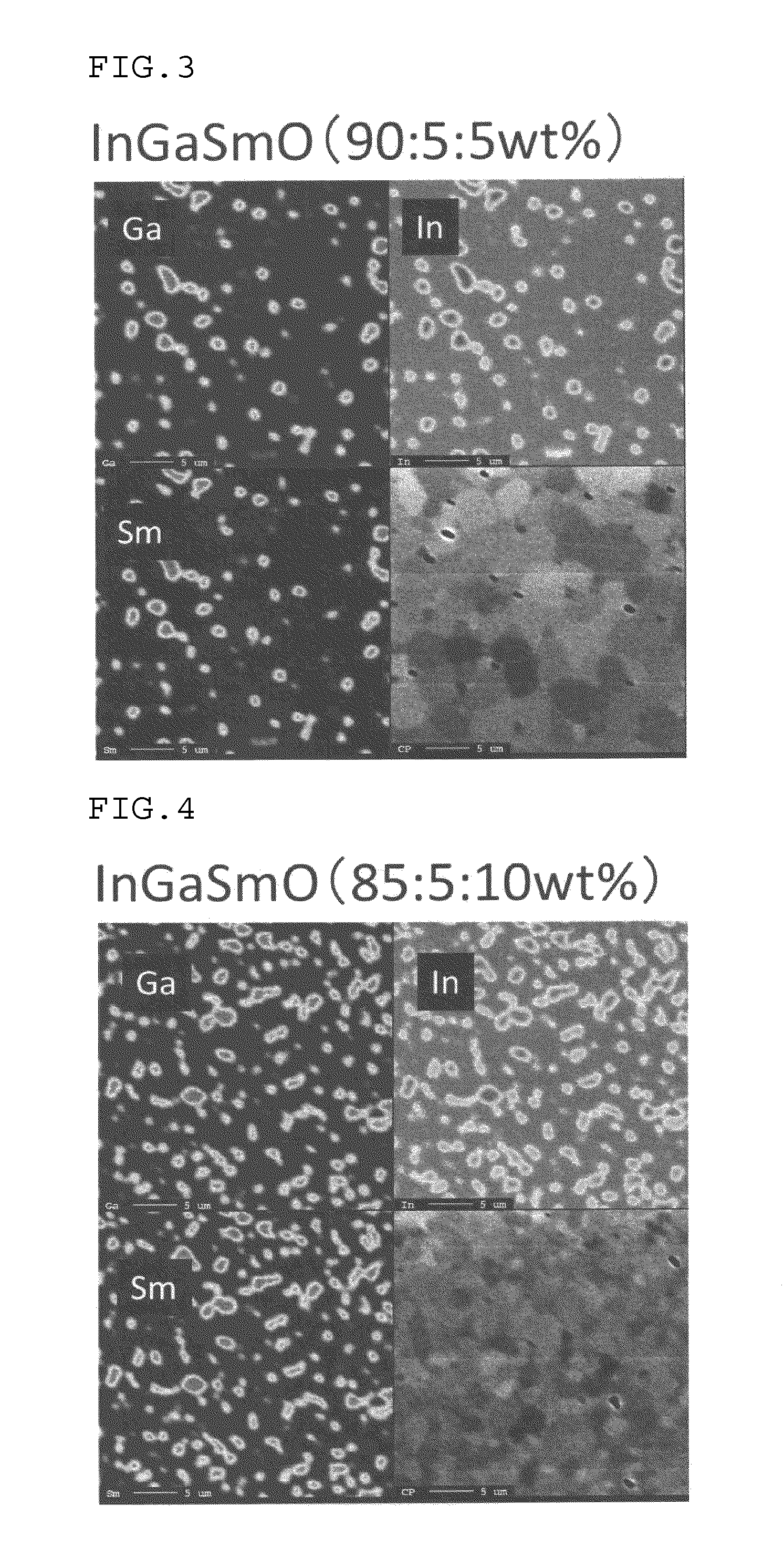
[0097]As raw material powders, the following oxide powders were used. The average particle size of the oxide powder was measured by a laser diffraction particle size analyzer SALD-300V (manufactured by Shimadzu Corporation). The median size D50 was employed as an average particle size for the following oxide powders.

[0098]Indium oxide powder: average particle size 0.98 μm

[0099]Gallium oxide powder: average particle size 0.96 μm

[0100]Aluminum oxide powder: average particle size 0.96 μm

[0101]Tin oxide powder: average particle size 0.95 μm

[0102]Samarium oxide powder: average particle size 0.99 μm

[0103]Yttrium oxide powder: average particle size 0.98 μm

[0104]Neodymium oxide powder: average particle size 0.98 μm

[0105]Gadolinium oxide powder: average particle size 0.97 μm

[0106]The above-mentioned oxide powders were weighed such that the oxide weight ratios shown in Tables 1 and 2 were attained. The weighed oxide powders were homogenously and finely pulverized an...


PUM

PropertyMeasurementUnit
particle sizeaaaaaaaaaa
crystallization temperatureaaaaaaaaaa
particle sizeaaaaaaaaaa

Abstract

An oxide sintered body comprising a bixbyite phase composed of In2O3 and an A3B5O12 phase (wherein A is one or more elements selected from the group consisting of Sc, Y, La, Ce, Pr, Nd, Pm, Sm, Eu, Gd, Tb, Dy, Ho, Er, Tm, Yb and Lu, and B is one or more elements selected from the group consisting of Al and Ga).

Description

TECHNICAL FIELD[0001]The invention relates to an oxide sintered body used as a raw material for obtaining an oxide semiconductor thin film of a thin film transistor (TFT) used in a display or the like such as a liquid crystal display or an organic EL display by a vacuum film forming process such as a sputtering method, a production method thereof, a sputtering target and a thin film transistor obtained therefrom.BACKGROUND ART[0002]Since an amorphous oxide semiconductor used in a TFT has a higher carrier mobility as compared with general-purpose amorphous silicon (a-Si), has a large optical band gap and can be formed at low temperatures, the application thereof in a next-generation display that requires an increase in size, high resolution and high-speed driving or a resin substrate having low heat resistance or the like is hoped for. In forming the above-mentioned oxide semiconductor (film), a sputtering method in which a sputtering target composed of the same material as that of t...

Claims


Application Information

Patent Timeline
Patent Type & Authority Applications(United States)
IPC IPC(8): H01J37/34C23C14/34H01L29/786C23C14/08C04B35/01C04B35/64
CPCH01J37/3429C04B2235/6567C04B35/64H01L29/7869C23C14/086C23C14/083C23C14/08C23C14/3414C04B2235/3286C04B2235/3222C04B2235/3224C04B2235/3225C04B2235/3229C04B2235/602C04B35/01H01J37/3426H01J37/3491H01L21/02565H01L21/02631C04B2235/3217C04B2235/3293C04B2235/5445C04B2235/764C04B2235/786C04B2235/80C04B2235/3227C04B2235/604C04B2235/6562C04B2235/762H01L29/66969
Inventor TOMAI, SHIGEKAZUINOUE, KAZUYOSHIEBATA, KAZUAKISHIBATA, MASATOSHIUTSUNO, FUTOSHITSURUMA, YUKIISHIHARA, YU
Owner IDEMITSU KOSAN CO LTD
Why Eureka
Try Eureka