

Palladium (PD)-coated copper wire for ball bonding
a technology of copper wire and coating, applied in the direction of metal-working apparatus, metallic material coating process, solid-state devices, etc., can solve the problem of difficult to leave the fine particles of palladium (pd) and achieve the effect of preventing the formation of al—cu intermetallic compounds, preventing the attachment of wires, and facilitating the unwinding of wires
- Summary
- Abstract
- Description
- Claims
- Application Information
AI Technical Summary
Benefits of technology
Problems solved by technology
Method used
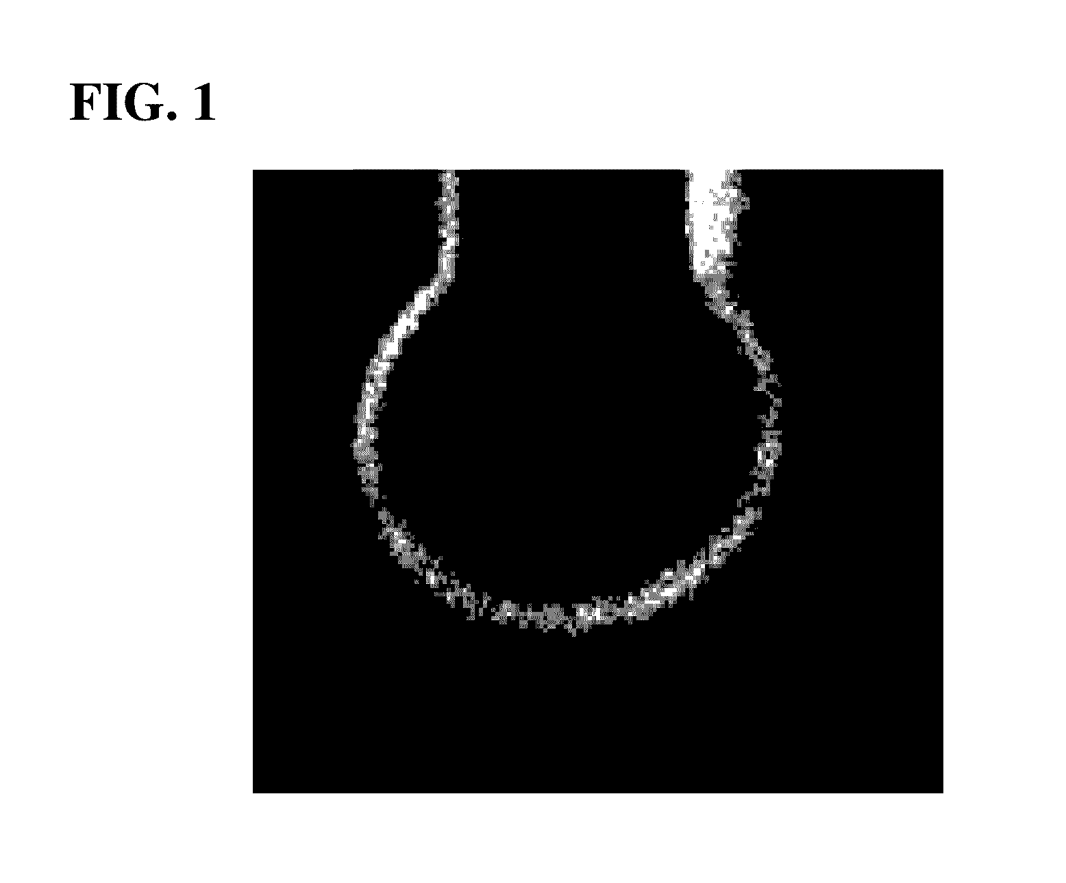
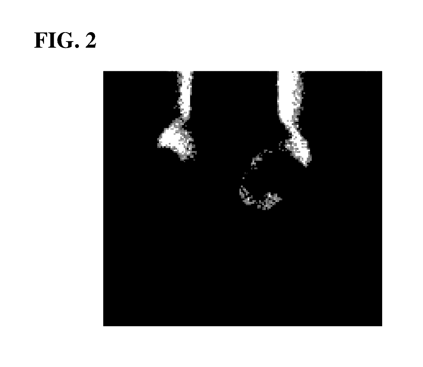
Image

Examples
examples
[0049]As the core, a core obtained by adding platinum (Pt), nickel (Ni) or phosphorus (P) to copper (Cu) whose purity was 99.9999% by mass or more or a core without the addition was used, and the core was continuously cast, was rolled while subjecting to previous heat processing, was thereafter primarily drawn into a wire, with the result that a thick wire (diameter of 1.0 mm) was obtained.
[0050]Then, a palladium (Pd) drawn layer and a gold (Au) ultra-thin drawn layer shown in table 1 were prepared, and the outer circumference of the thick wire was coated with them. The purity of the gold (Au) in the ultra-thin drawn layer was 99.99% by mass or more, and the purity of the palladium (Pd) was 99.9% by mass or more.
examples 1 to 3
[0051]A coating layer of a palladium (Pd)-sulfur (S) amorphous alloy was formed as follows. To a commercially available palladium (Pd) electroplating bath (ADP700 made by Japan Electro Plating Co., Ltd.), 0.1 g / L, 0.005 g / L and 0.15 g / L of ADP700 additive made by the company were individually added, and thus the concentration of sulfur (S) in the plating bath was set medium, low and high. In this plating bath, a current whose current density was 0.75 A / dm2 was passed through the copper wire having the diameter of 1.0 mm, and the coating layer of the palladium (Pd)-sulfur (S) amorphous alloy was formed. These three types coated copper wires were coated with gold (Au) by magnetron sputtering such that the gold (Au) had a predetermined thickness.
[0052]Thereafter, baking processing was not performed, continuous secondary wire drawing was performed under wet conditions with a diamond die, refining heat processing was performed at 480° C. for one second and palladium (Pd)-coated copper wi...
example 4
[0053]A coating layer of a palladium (Pd)-phosphorus (P) amorphous alloy was formed as follows. To a commercially available palladium (Pd) electroless plating bath (ADP700 made by Japan Electro Plating Co., Ltd.), 0.2 g / L of phosphorous acid (H3PO3) was added. In this plating bath, a current whose current density was 0.75 A / dm2 was passed through the copper wire having a diameter of 1.0 mm, and the coating layer of the palladium (Pd)-phosphorus (P) amorphous alloy was formed. Thereafter, as with example 1, a palladium (Pd)-coated copper wire for ball bonding in example 4 was manufactured.
PUM
| Property | Measurement | Unit |
|---|---|---|
| diameter | aaaaa | aaaaa |
| thickness | aaaaa | aaaaa |
| thickness | aaaaa | aaaaa |
Abstract
Description
Claims
Application Information