3D Bendable Printed Circuit Board With Redundant Interconnections

a printed circuit board and redundant technology, applied in the direction of printed circuit non-printed electric component association, printed element electric connection formation, etc., can solve the problems of failure modes in the pcb, not considered good a good solution for bendable or wearable applications, and thick copper becomes extremely rigid and incurs high stress between the copper and the pcb

Active Publication Date: 2017-04-27
ADVENTIVE INT LTD
View PDF6 Cites 45 Cited by
  • Summary
  • Abstract
  • Description
  • Claims
  • Application Information

AI Technical Summary

Benefits of technology

[0068]In an alternative method, no rigid conductive layer or PCB conductive layer is used. Instead a “quasi PCB” is formed by printing with a movable print head a relatively thick layer of, for example, a polymeric material or polyimide compound, onto the flexible protective cap layer in areas where “quasi PCBs” are to be located. Openings may be left in the relatively thick layer where vias to the flexible conductive layer are to be formed, and a thinner layer of the same material may be printed onto areas where the flexible PCB are to be located. The thickness of the thinner layer may be calibrated such that an etching process removes the thinner layer while a via is formed in the flexible protective cap layer, exposing the flexible conductive layer, eliminating the need for photomasking. The movable print head may then be used to print a patterned layer of conductive material onto the relatively thick layer and to fill the via and contacting the flexible conductive layer.
[0069]Whichever method is used to form the PCBs or quasi-PCBs and flexible PCBs, electronic or other component are then mounted onto the PCBs or quasi-PCBs and the electronic system is protected against mechanical damage, moisture, and other environmental conditions.

Problems solved by technology

One disadvantage of rigid PCBs is they are intrinsically planar and cannot bend to fit curved surfaces.
As such they are not considered good a good solution for bendable or wearable applications.
Thick copper becomes extremely rigid and incurs high stress between the copper and the PCB resulting from differences in the TCE, i.e. the temperature coefficient of expansion, of the dissimilar materials.
Extreme stress can lead to a variety of failure modes in a PCB, including board cracking, delamination of the conductive layers, and solder joint cracking.
Because the photoresist comprises an organic compound, it is relatively insensitive to exposure to acids, especially after hard baking.
Although an entire electronic system can be integrated onto a single rigid PCB, in many instances, the resulting PCB is too large or has the wrong shape to fit in available space.
In reality, however, the wiring from board-to-board introduces parasitic resistance, capacitance, and inductance that can distort sensitive analog signals, interfere with radio frequency (RF) communication, emit electromagnetic interference (EMI), and limit data communication and clock rates to low frequency operation.
These parasitic elements also can adversely impact power distribution and affect voltage regulation accuracy or stability.
Moreover, because the flexible pads are positioned in various locations across a patient's body, normal application of the product repeatedly subjects the cable to movement, twisting and pulling.
Despite these precautions, electrical connections subjected to repeated flexing, bending, and wire-pull exhibit poor long-term survivability and suffer frequent reliability failures.
As a result these defective or weak solder joints exhibits disproportionately higher failure rates than good solder joint 50, especially when subjected to wire pull.
In applications with repeated movement and flexing, plug and socket connections suffer several failure modes—the most common failure comprising a case where the plug comes loose from the socket and no longer makes a reliable connection between the plug pins and the socket's conductors.
Unfortunately, clamping sockets eliminate one failure mode but introduce a new failure mode in the cable.
Specifically, if the plug is held tightly in place, during movement, twisting, or pulling, the connection between the ribbon cable and the plug will fail.
Regardless of whether repeated movement or flexing results in an unplugged connector or a broken cable, the interconnection between PCBs will fail and an open circuit will result.
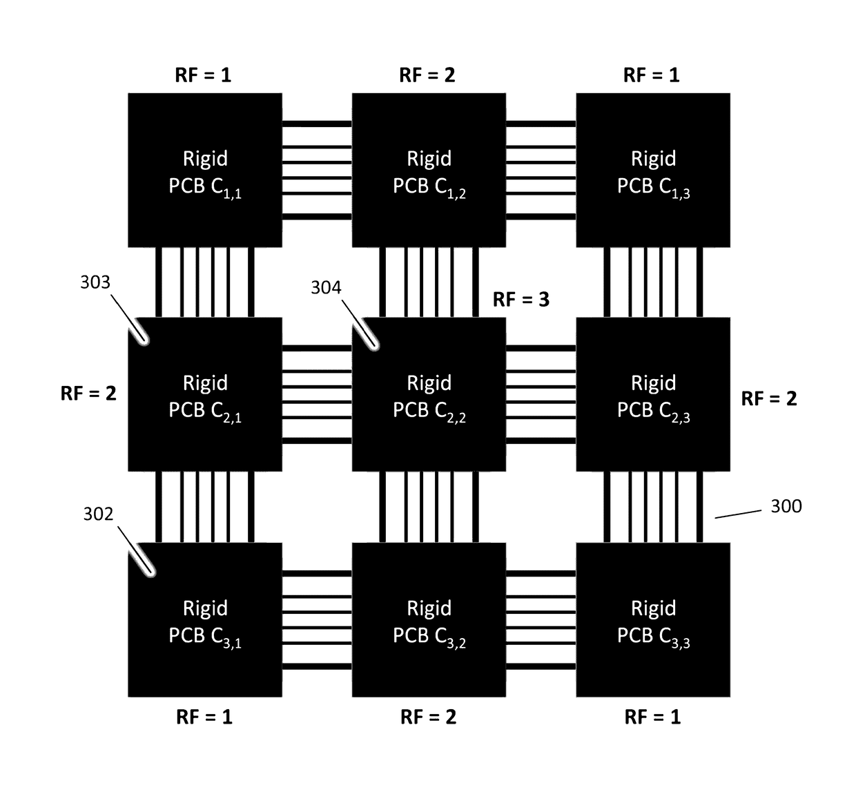
In systems comprising a large number of rigid PCBs, e.g. in a series of PCB's used to cover a large area, the number of interconnections further exacerbates the problem with each connector statistically increasing the probability of system failure.
While the use of ribbon cable and their associated plugs and connectors reduce the risk of system failure from wired connection failure-modes such as wire pull or solder joint cracking, ribbon cable is still subject to single point system failure, i.e. where a single wire break results in partial or total system malfunction.
For example, if a control wire is broken, the system will not be able to receive commands.
In cases where two wires are required to carry the required current, breakage of either wire will cause a single wire to carry too much current leading to excessive voltage drops, overheating, instantaneous wire fusing, or electromigration failure over time.
Insuring PCB connection reliability is especially problematic in applications subject to repeated cycles of flexing.
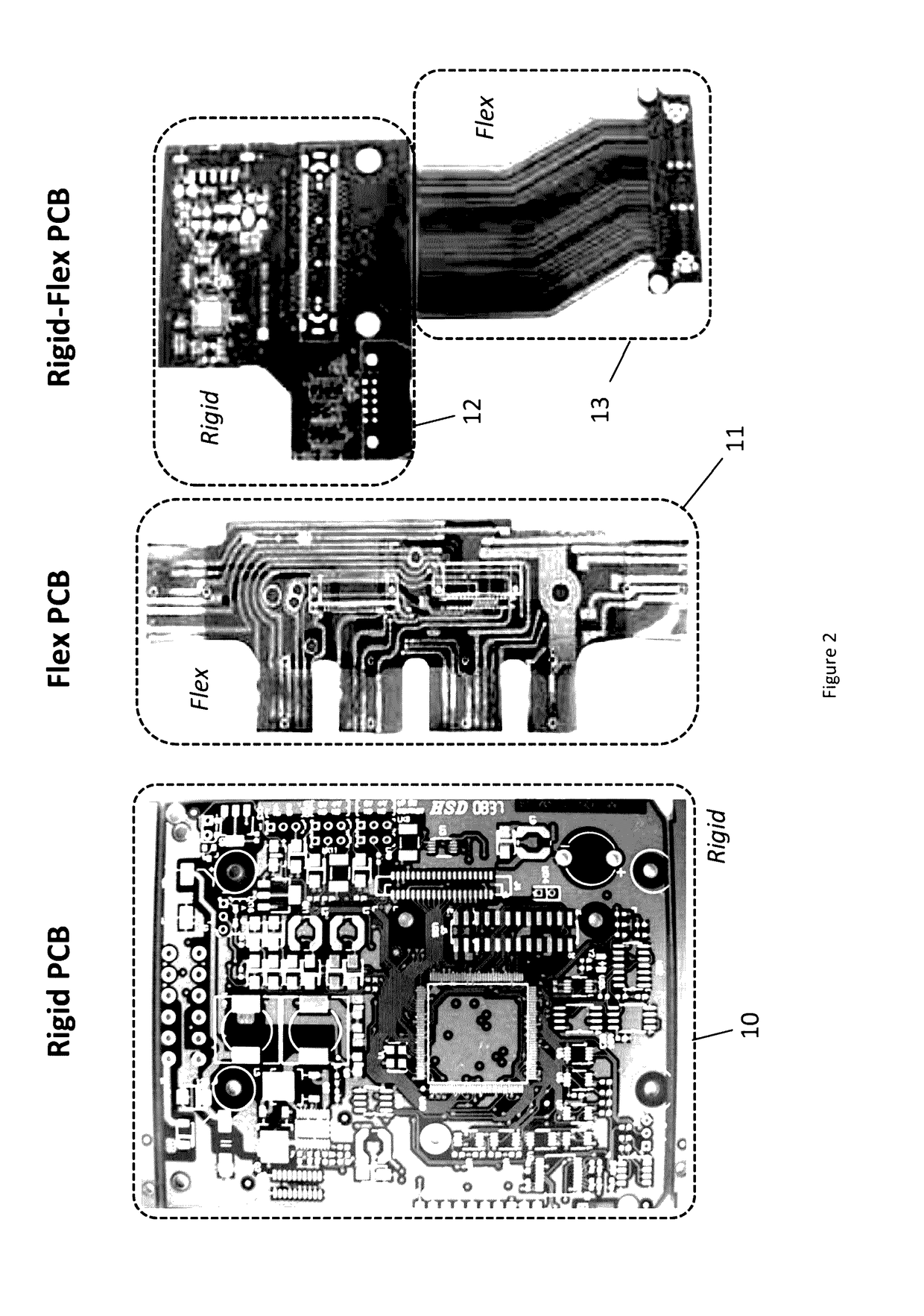
As described, flex PCBs are limited to “rarely-flexed” applications because of the mismatch between the flexible PCB and the rigid components mounted on it.
The problematic use of flex circuits, i.e. flex PCBs with mounted components in applications with repeated flexing cycles, damage and breakage occurs because the components themselves do not bend even though the PCB does.
By subjecting the PCB to larger stresses or additional flexing cycles, the size of the crack will grow larger.
Cracking can also occur on solder joints mounting passive components such as resistors and capacitors.
The combination of rigid and flex PCBs further exacerbates the problem by requiring connections between the two.
Such connections are subject to the same socket-plug failures as ribbon cables described previously.
The main disadvantage is due to the mismatch in mechanical properties between the rigid and flex layers, it is easy to rip the flex PCB by any force applied perpendicular to the plane created by the PCBs near the bar shaped interconnection area, i.e. in the z-direction as illustrated in drawing 170 of FIG. 12A where rigid PCB 171 connects to flex PCB 173 along a thin bar shared intersection expanded in cross section 173.
Multi-PCB System Failure
From an electronics system perspective however, such distributed circuits, i.e. ones where pieces of the circuit are implemented on different PCBs, suffer from numerous system reliability risks associated with communication among the various components.
In such distributed systems, tear 193 to flex PCB 191B may not just sever rigid PCB 190C from the rest of the system but likely can cause the entire system to malfunction or the software to crash.
Such distributed systems are sensitive to single point failures and offer little or no protection from mechanical damage to the interconnections between its multiple rigid PCBs.
By contrast, in distributed electronic system 189C also in FIG. 13B, tear 194C in the flex PCB results in an open circuit in one or more conductors carrying control signals 193B resulting in system malfunction, affecting normal operation and depending on the function of the interrupted signals, possibly resulting in a total system failure.
Moisture & Corrosion Failures
Another physical mechanism that may result in immediate or gradual system malfunction is moisture-induced electrical failure.
In the event that a PCB is immersed in or subjected to any conductive or slightly conductive fluid, an electrical short may result, either impairing or potentially damaging a circuit or system.
In wearable electronics, circuitry and PCBs may also be subjected to rain and to body sweat.
Sweat is especially problematic because it contains salt and other electrolytes making it more electrically conductive.
Failures may comprise electrical shorts or because of corrosion may also result in electrical open circuits.
Coating flex PCBs with a protective layer is problematic because the coating invariably cracks with repeated flexing.
Coating rigid PCBs is beneficial but does not support bendable or wearable PCB applications.

Method used


Image

  • 3D Bendable Printed Circuit Board With Redundant Interconnections
  • 3D Bendable Printed Circuit Board With Redundant Interconnections
  • 3D Bendable Printed Circuit Board With Redundant Interconnections

Examples


Embodiment Construction

[0342]As described previously, realizing electronic circuits and systems generally involves mounting and interconnecting electronic components on printed circuit boards or PCBs. Such PCBs comprise either rigid PCBs that cannot bend or change shape, flex type PCBs that can flex or twist, or combinations thereof. In medical devices such as LED light pads used in phototherapy or in sports applications such wearable electronics or “wearables” all of the aforementioned technologies suffer from numerous disadvantages. Rigid PCBs break or crack if bent, components mounted on flex PCBs fall off from solder cracking after repeated flexing cycles, and hybrid rigid-flex PCBs tear or rip where the flex PCB connects to the rigid PCBs. Other methods to interconnect rigid PCBs using wire or connectors likewise result in partial or total electrical failure of the electronic system after repeated bending of the PCBs and their interconnections. In many cases breakage or moisture induced corrosion of ...


PUM


Abstract

A rigid-flex PCB includes an array of rigid PCB “islands” interconnected by a flexible PCB formed into flexible connectors. The conductive and insulating layers of the flexible PCB extend into the rigid PCBs, giving the electrical connections to the rigid PCBs added resistance to breakage as the rigid-flex PCB is repeatedly stressed by bending and twisting forces. In addition, the durability of the rigid-flex PCB is enhanced by making the power and signal lines driving the rigid PCBs redundant so that a breakage of a line will not necessarily affect the operation of the rigid PCB to which it is attached. The rigid-flex PCB is particularly applicable to light pads used in phototherapy, wherein LEDs mounted on the rigid-PCBs are powered and controlled through the redundant lines in the flexible PCB.

Description

FIELD OF THE INVENTION[0001]This invention relates to bendable printed circuit boards with low failure rates during use including methods and apparatus designed for their manufacturing and applications.BACKGROUND OF THE INVENTION[0002]Printed circuit boards (PCBs) comprise one or more layers of conductors, typically copper, separated by insulting layers such as glass, epoxy, or polyimide on which electronic components are physically mounted, providing mechanical support for electronic circuitry. By soldering components' leads onto the PCB's conductive traces, electronic devices such as integrated circuits, transistors, diodes, resistors, capacitors, inductors, and transformers are electrically interconnected to form electronic circuits. Applications of PCBs include virtually every type of electronic product including cell phones, cameras, lithium ion batteries, tablet computers, notebooks, desktops, servers, network equipment, radios, consumer devices, televisions, set top boxes, in...

Claims


Application Information

Patent Timeline
Patent Type & Authority Applications(United States)
IPC IPC(8): H05K1/14H05K3/40H05K3/02H05K3/32H05K3/06H05K3/00H05K3/36H05K3/18
CPCH05K1/148H05K1/147H05K3/361H05K3/4038H05K3/188H05K3/32H05K2203/1327H05K3/0026H05K3/027H05K2201/056H05K2201/058H05K2201/2009H05K2201/10106H05K3/061H05K1/11H05K1/18H05K1/0266H05K1/0268H05K3/4691H05K3/0035H05K2201/052H05K2201/09245H05K2201/09254H05K2201/0979H05K3/06H05K3/24
Inventor WILLIAMS, RICHARD K.LIN, KENG HUNG
Owner ADVENTIVE INT LTD
Why Eureka
Try Eureka