Systems And Methods For Extended Infrared Spectroscopic Ellipsometry

a technology of infrared spectroscopic ellipsometry and extended infrared, which is applied in the direction of optical radiation measurement, semiconductor/solid-state device testing/measurement, instruments, etc., can solve the problem that many available high-throughput metrology techniques are unable to reliably perform cd and film measurements of high aspect ratio structures, and many optical techniques suffer from low signal-to-noise ratios (snrs), so as to achieve small

Active Publication Date: 2017-07-20
KLA TENCOR TECH CORP
View PDF0 Cites 24 Cited by
  • Summary
  • Abstract
  • Description
  • Claims
  • Application Information

AI Technical Summary

Benefits of technology

[0010]Methods and systems for performing simultaneous spectroscopic measurements of semiconductor structures at ultraviolet, visible, and infrared wavelengths are presented herein. Spectra including ultraviolet, visible, and infrared wavelengths are measured at high throughput with the same alignment conditions. In this manner, machine errors, such as wavelength errors, are uniformly corrected across all measured wavelengths. By simultaneously measuring a target with infrared, visible, and ultraviolet light in a single system, precise characterization of complex three dimensional structures is

Problems solved by technology

Such high aspect ratio structures create challenges for film and CD measurements.
Many optical techniques suffer from low signal-to-noise ratios (SNRs), as only a small fraction of the illumination light is able to reach the bottom of high aspect ratio features, and reflect upwards to the detector.
Thus, many available high-throughput metrology techniques are unable to reliably perform CD and film measurements of high aspect ratio structures.
Cross-sectional scanning electron microscopy (SEM) is a low throughput, destructive technique that is not suitable for inline metrology.
Atomic force microscopy (AFM) is limited in its ability to measure high aspect ratio structures and has relatively low throughput.
CD-SAXS has not yet been demonstrated to achieve high throughput capabilities required by the semiconductor industry.
Model based infrared reflectometry (MBIR) has been used for metrology of high aspect ratio DRAM structures, but the technique lacks the resolution provided by shorte

Method used


Image

  • Systems And Methods For Extended Infrared Spectroscopic Ellipsometry
  • Systems And Methods For Extended Infrared Spectroscopic Ellipsometry
  • Systems And Methods For Extended Infrared Spectroscopic Ellipsometry

Examples


Embodiment Construction

[0029]Reference will now be made in detail to background examples and some embodiments of the invention, examples of which are illustrated in the accompanying drawings.

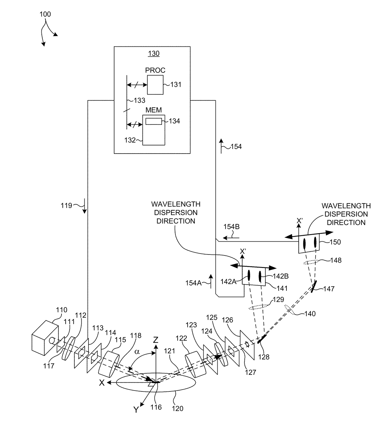
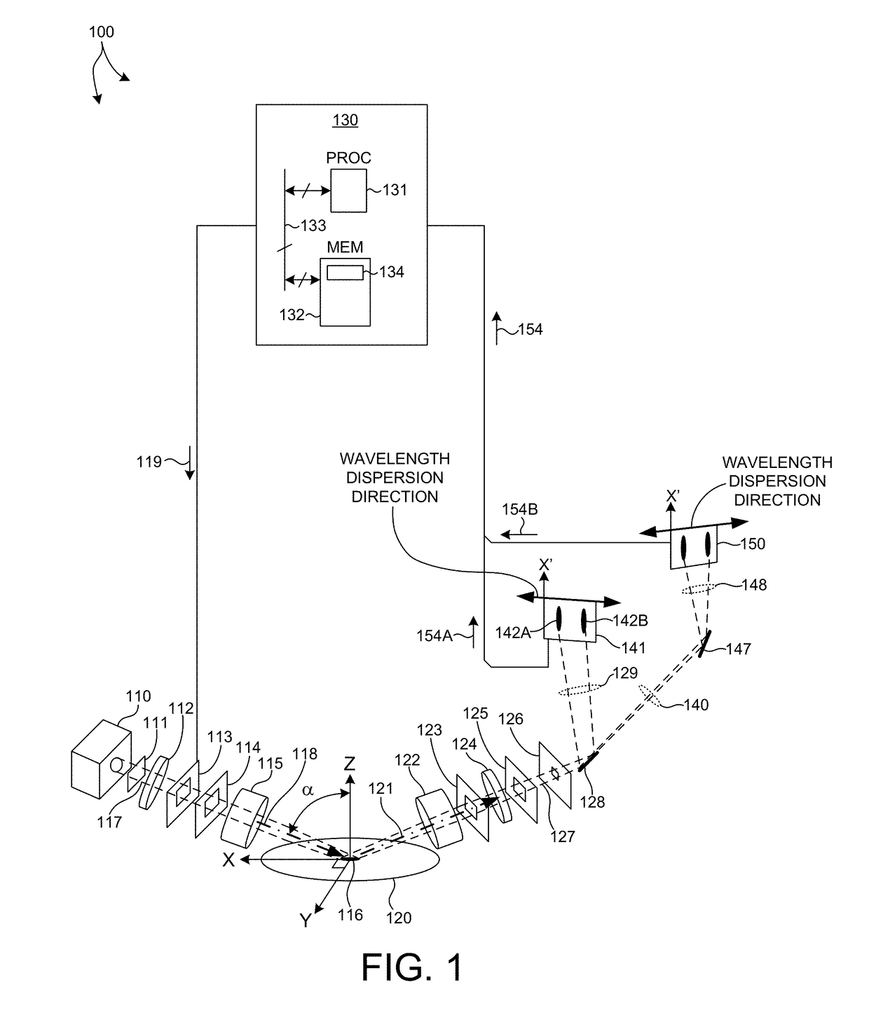
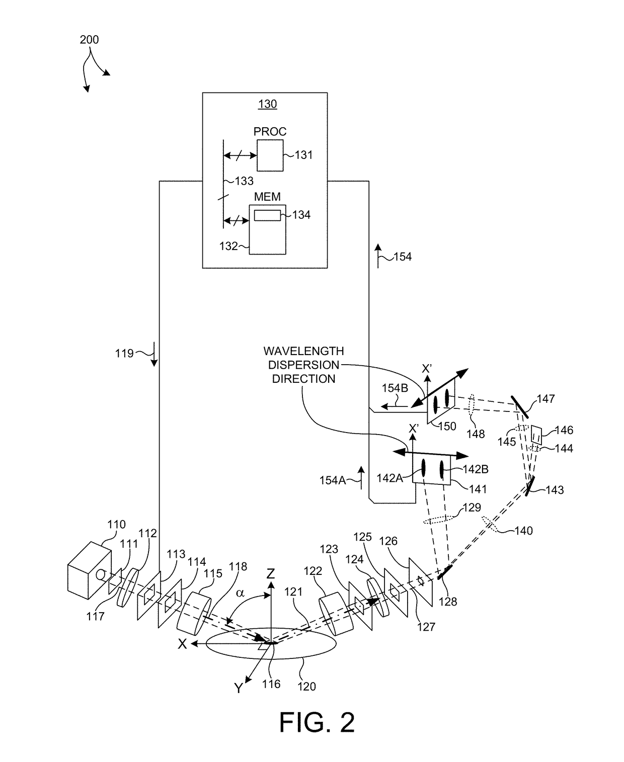
[0030]Methods and systems for performing simultaneous spectroscopic measurements of semiconductor structures at ultraviolet, visible, and infrared wavelengths are presented herein. Spectra including ultraviolet, visible, and infrared wavelengths are measured at high throughput with the same alignment conditions. In this manner, machine errors, such as wavelength errors, are uniformly corrected across all measured wavelengths. In another aspect, wavelength errors are reduced by orienting the direction of wavelength dispersion on the detector surface perpendicular to the projection of the plane of incidence onto the detector surface. In another aspect, a broad range of infrared wavelengths are detected by a detector that includes multiple photosensitive areas having different sensitivity characteristics. Collected light...


PUM


Abstract

Methods and systems for performing simultaneous spectroscopic measurements of semiconductor structures at ultraviolet, visible, and infrared wavelengths are presented herein. In another aspect, wavelength errors are reduced by orienting the direction of wavelength dispersion on the detector surface perpendicular to the projection of the plane of incidence onto the detector surface. In another aspect, a broad range of infrared wavelengths are detected by a detector that includes multiple photosensitive areas having different sensitivity characteristics. Collected light is linearly dispersed across the surface of the detector according to wavelength. Each different photosensitive area is arranged on the detector to sense a different range of incident wavelengths. In this manner, a broad range of infrared wavelengths are detected with high signal to noise ratio by a single detector. These features enable high throughput measurements of high aspect ratio structures with high throughput, precision, and accuracy.

Description

CROSS REFERENCE TO RELATED APPLICATION[0001]The present application for patent claims priority under 35 U.S.C. §119 from U.S. provisional patent application Ser. No. 62 / 279,469, entitled “Apparatus and Methods of Extended Infrared Ellipsometry,” filed Jan. 15, 2016, the subject matter of which is incorporated herein by reference in its entirety.TECHNICAL FIELD[0002]The described embodiments relate to metrology systems and methods, and more particularly to methods and systems for improved measurement of three dimensional semiconductor structures.BACKGROUND INFORMATION[0003]Semiconductor devices such as logic and memory devices are typically fabricated by a sequence of processing steps applied to a specimen. The various features and multiple structural levels of the semiconductor devices are formed by these processing steps. For example, lithography among others is one semiconductor fabrication process that involves generating a pattern on a semiconductor wafer. Additional examples of...

Claims


Application Information

Patent Timeline
IPC IPC(8): G01N21/3563G01J3/18G01J3/427G01N21/21
CPCG01N21/3563G01N21/211G01J2003/4275G01J3/427G01N2021/3568G01J3/18G01J3/2803G01J3/36G01N21/31G01N21/9501G01N2021/213G01J3/0224G03F7/70616H01L22/12H01L22/24
Inventor KRISHNAN, SHANKARWANG, DAVID Y.
Owner KLA TENCOR TECH CORP
Why Eureka
Try Eureka