Copper electroplating baths and electroplating methods capable of electroplating megasized photoresist defined features

Active Publication Date: 2017-10-05
ROHM & HAAS ELECTRONIC MATERIALS LLC
View PDF2 Cites 2 Cited by
  • Summary
  • Abstract
  • Description
  • Claims
  • Application Information

AI Technical Summary

Benefits of technology

The patent discusses a method and bath for coating copper onto semiconductors. This method results in coated semiconductors with uniform and smooth surface profiles, without any bumps or uneven areas. The method allows for the creation of copper features with a smooth and flat profile, making them ideal for use in electronic devices. The combination of two specific chemicals is used to create the desired coating, resulting in a highly-efficient and effective process. Overall, this patent provides a way for creating finely-detailed copper coatings on semiconductors, allowing for improved performance and reliability in electronic devices.

Problems solved by technology

However, development of such plating chemistry and method is a challenge for the industry as improvement in one attribute typically comes at the expense of another.
At such high plating rates pillars electroplated from many conventional copper electroplating baths develop nodule defects and irregular surface morphology.
Such nodule defects and irregular surface morphology can compromise performance of electronic articles in which the pillars are included.

Method used


Image

  • Copper electroplating baths and electroplating methods capable of electroplating megasized photoresist defined features
  • Copper electroplating baths and electroplating methods capable of electroplating megasized photoresist defined features
  • Copper electroplating baths and electroplating methods capable of electroplating megasized photoresist defined features

Examples


example 1

[0058]In 250 mL round-bottom, three-neck flask equipped with a condenser and a thermometer, 100 mmol of 2-aminobenzoic acid and 20 mL of deionized (“DI”) water were added followed by addition of 100 mmol of aqueous sodium hydroxide at room temperature and 100 mmol of 1,4-butanediol diglycidyl ether at 80° C. The resulting mixture was heated for about 5 hours using an oil bath set to 95° C. and then left to stir at room temperature for additional 6 hours. The reaction product (Reaction Product 1) was transferred into a container, rinsed and adjusted with DI water. The reaction product solution was used without further purification.

example 2

[0059]In 100 mL round-bottom, three0neck flask equipped with a condenser and a thermometer, 100 mmol of 2H-imidazole and 20 mL of DI water were added followed by addition of 100 mmol of epichlorohydrin. The resulting mixture was heated for about 5 hours using an oil bath set to 110° C. and then left to stir at room temperature for an additional 8 hours. An amber colored not-very viscous reaction product was transferred to a 200 mL volumetric flask, rinsed and adjusted with DI water to the 200 mL mark. The reaction product (Reaction Product 2) solution was used without further purification.

example 3

[0060]An aqueous acid copper electroplating bath was prepared by combining 60 g / L copper ions from copper sulfate pentahydrate, 60 g / L sulfuric acid, 90 ppm chloride ion, 12 ppm of an accelerator and 2 g / L of a suppressor. The accelerator was bis(sodium-sulfopropyl)disulfide. The suppressor was an EO / PO copolymer having a weight average molecular weight of around 1,000 and terminal hydroxyl groups. The electroplating bath also contained 10 ppm of Reaction Product 1 and 3 ppm of Reaction Product 2. The pH of the bath was less than 1.

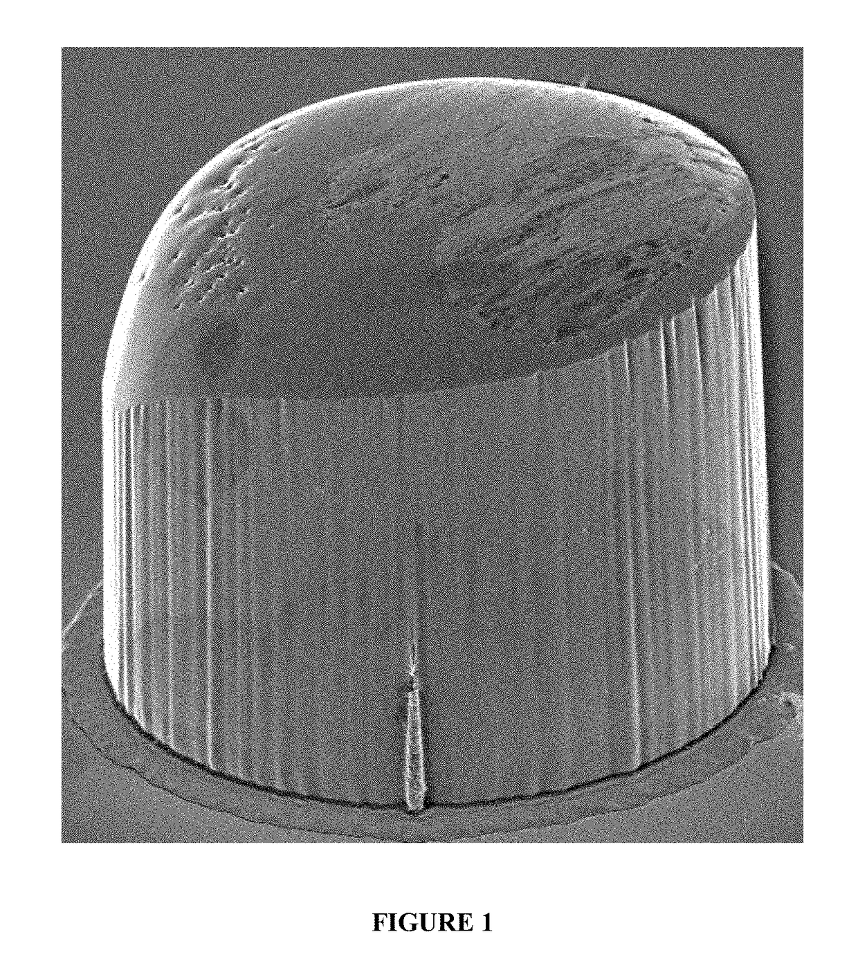
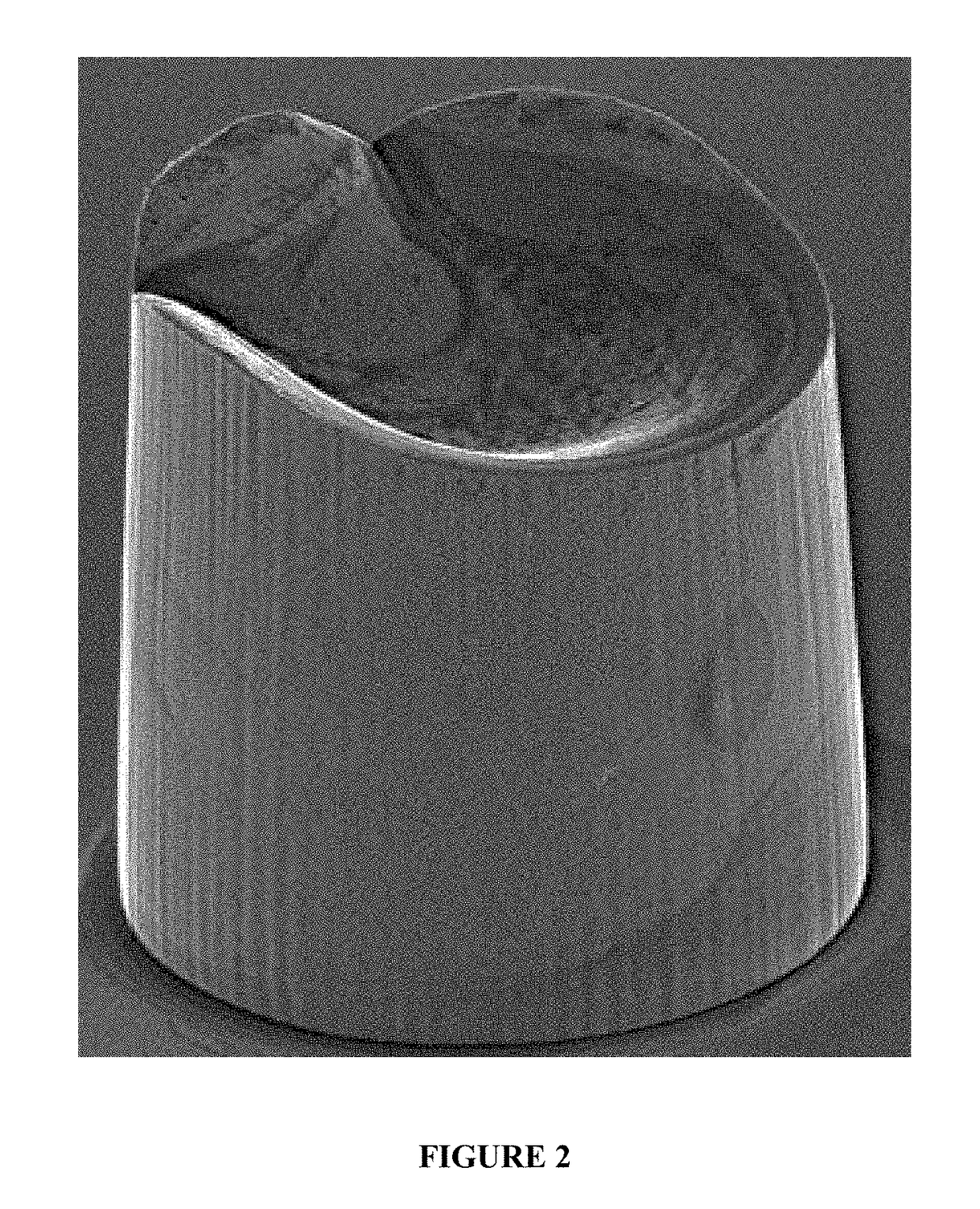
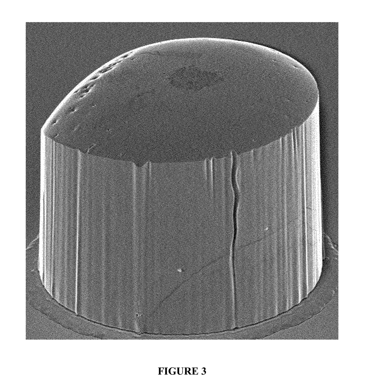
[0061]A 300 mm silicon wafer segment with a patterned photoresist 240 μm thick and a plurality of vias (available from IMAT, Inc., Vancouver, Wash.) was immersed in the copper electroplating bath. The anode was a soluble copper electrode. The wafer and the anode were connected to a rectifier and copper pillars were electroplated on the exposed seed layer at the bottom of the vias. The via diameters were 200 μm. Current density during plating was 30 ASD an...


PUM

PropertyMeasurementUnit
Fractionaaaaaaaaaa
Fractionaaaaaaaaaa
Fractionaaaaaaaaaa

Abstract

Copper electroplating baths and methods enable the plating of photoresist defined megafeatures at high current densities which have substantially uniform morphology and reduced nodule development. The copper electroplating baths include a mixture of heterocyclic nitrogen containing copolymers which provide megafeatures having a good % TIR and % WID balance.

Description

FIELD OF THE INVENTION[0001]The present invention is directed to copper electroplating baths and electroplating methods capable of electroplating megasized photoresist defined features. More specifically, the present invention is directed to copper electroplating baths and electroplating methods capable of electroplating megasized photoresist defined features where the megasized photoresist defined features have substantially uniform surface morphology.BACKGROUND OF THE INVENTION[0002]Photoresist defined features include copper pillars and redistribution layer wiring such as bond pads and line space features for integrated circuit chips and printed circuit boards. The features are formed by the process of lithography where a photoresist is applied to a substrate such as a semiconductor wafer chip often referred to as a die in packaging technologies, or epoxy / glass printed circuit boards. In general, the photoresist is applied to a surface of the substrate and a mask with a pattern i...

Claims


Application Information

Patent Timeline
IPC IPC(8): C25D5/02C25D3/38
CPCC25D3/38C25D5/022C25D7/00C25D7/123C25D21/12G03F7/0002
Inventor THORSETH, MATTHEWHAZEBROUCK, REBECCASCALISI, MARKNIAZIMBETOVA, ZUHRADZIEWISZEK, JOANNA
Owner ROHM & HAAS ELECTRONIC MATERIALS LLC
Why Eureka
Try Eureka