GaN-on-Si SEMICONDUCTOR DEVICE STRUCTURES FOR HIGH CURRENT/ HIGH VOLTAGE LATERAL GaN TRANSISTORS AND METHODS OF FABRICATION THEREOF

a technology of gan-on-si semiconductor and gan-on-si, which is applied in the direction of basic electric elements, electrical equipment, inorganic chemistry, etc., can solve the problems of significant interlayer stress/strain and wafer bowing, cracking during fabrication, and subsequent defect related reliability problems

Active Publication Date: 2018-01-11
GAN SYST
View PDF1 Cites 18 Cited by
  • Summary
  • Abstract
  • Description
  • Claims
  • Application Information

AI Technical Summary

Benefits of technology

[0017]The present invention seeks to provide improved structures and methods of fabrication of nitride semiconductor devices, such as GaN power transistors and systems comprising one or more lateral GaN power transistors, which addresses at least one of the above-mentioned problems, or at least provides an alternative.

Problems solved by technology

However, the thermal and lattice mismatch between the GaN semiconductor layers and the silicon surface tends to cause significant interlayer stresses / strains and wafer bowing when using large scale wafers.
The thermal and lattice mismatch and the resulting interlayer stresses / strains between the GaN epi-layers and the silicon substrate introduces defects, such as misfit dislocations, which can potentially lead to cracking during fabrication and subsequent defect related reliability issues.
One significant issue is cracking or propagation of defects in the GaN epi-layers during wafer dicing to separate individual die.
For example, it has been observed that wafer dicing using conventional mechanical sawing, i.e. blade dicing with a diamond saw, can cause dicing damage that seeds cracks in the GaN epi-layers.
If these cracks are not detected in final test, the cracks can subsequently propagate into active areas of the device and cause reliability issues.
However, it has been observed that laser grooving also creates surface damage and / or defects in the region of the substrate / GaN epi-layer interface.
Stealth dicing uses high power laser pulses, which create microscopic sub-surface damage to initiate controlled cleaving or splitting of the substrate wafer along the laser defined scribe line.
(Infineon), discusses limitations of plasma dicing and discloses that modern wafer dicing methods, such as plasma dicing offer advantages for some materials, but may not be suitable for cutting through other materials, e.g. thick metal layers such as back-side contact metallization layers.
However, for GaN-on-Si die, stealth dicing or other methods for inducing cleaving of the GaN epi-layers would lead to cracking and damage of the GaN-epilayers.
However, none of the above-mentioned references address issues of cracking or delamination of the GaN epi-layers during wafer dicing for singulation of large area GaN-on-Si die comprising high voltage / high current GaN power transistors.
For example, issues of poor yield and reliability caused by poor mechanical properties of low k dielectrics which can lead to dicing induced damage and may cause cracking of dielectric layers and delamination of metal and dielectric layers is discussed, for example, in United States Patent Application publication No.
However, such structures do not address issues with dicing induced cracking or defect creation in the active regions comprising GaN epi-layers on a silicon substrate, where thermal and lattice mismatch creates significant interlayer stresses / strains and misfit dislocations in the GaN epi-layers.
Thus, for GaN power devices with these large die sizes, interlayer stresses / strains between the GaN epi-layers and the silicon substrate can lead to cracking, and dicing induced damage can significantly reduce yield of good die, as well as compromise long term device reliability.

Method used


Image

  • GaN-on-Si SEMICONDUCTOR DEVICE STRUCTURES FOR HIGH CURRENT/ HIGH VOLTAGE LATERAL GaN TRANSISTORS AND METHODS OF FABRICATION THEREOF
  • GaN-on-Si SEMICONDUCTOR DEVICE STRUCTURES FOR HIGH CURRENT/ HIGH VOLTAGE LATERAL GaN TRANSISTORS AND METHODS OF FABRICATION THEREOF
  • GaN-on-Si SEMICONDUCTOR DEVICE STRUCTURES FOR HIGH CURRENT/ HIGH VOLTAGE LATERAL GaN TRANSISTORS AND METHODS OF FABRICATION THEREOF

Examples


first embodiment

[0089]FIG. 6 shows a simplified schematic cross-sectional diagram of part 300-1 of the GaN-on-Si wafer e.g. a cross-section through A-A of the structure shown in FIG. 5, through die 110 and parts of neighbouring die.

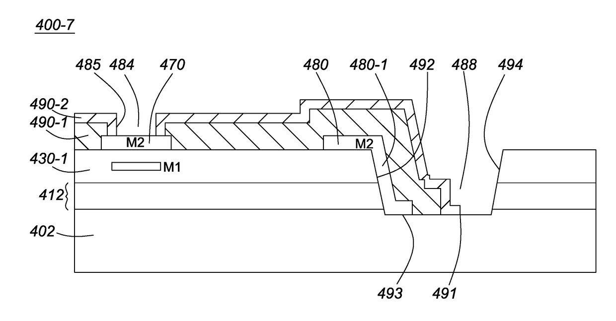
[0090]Many elements of FIG. 6 are similar to those of FIG. 3 and are labelled with the same part numbers incremented by 100. That is, each die 110 comprises a lateral GaN power transistor 314 formed on a silicon substrate 302. The GaN transistor structure 314 comprises a plurality of GaN epitaxial layers, i.e. GaN epi-layer stack 312. The GaN epi-layer stack 312 includes a GaN / AlGaN heterostructure providing a 2DEG active region 310. Source electrode S, drain electrode D and gate electrode G of the lateral GaN transistor are formed on the 2DEG active region 310. Also shown are overlying Back End of the Line (BEOL) layers 330, i.e. comprising first and second metallization layers M1 and M2, which define source contacts 332 and 334 and drain contacts 334 and 344, and inte...

second embodiment

[0093]FIG. 7 shows part of a device structure 300-2 which is similar to that shown in FIG. 6 and similar elements are labelled with the same reference numerals as in FIG. 6. Additionally, in the device structure of this embodiment, a trench cladding 390 (trench lining) comprising an edge sealing layer or protective layer, is provided on at least the inner or proximal side walls 392 of the pre-dicing trenches 388, surrounding each die. The trench cladding 390 may comprise one or more conformal dielectric layers, and optionally a metal layer, provided on the inner (proximal) sidewalls 392 of the trench, which seal any exposed edges of the epi-layer stack and overlying BEOL layers. In referring to inner sidewalls 392 of the trench 388, this means the sidewalls which are proximal to the centre of the die. The outer (distal) sidewalls 394 are closer to the edge of the die.

third embodiment

[0094]As illustrated in FIG. 8, in a device structure 300-3 the cladding 390 is provided as a conformal layer or layers extending over the surface of the GaN-on-Si die, and extending over inner sidewalls of the pre-dicing trenches. Other elements of the device structure shown in FIG. 8 are similar to those in FIGS. 6 and 7 and are labelled with the same reference numerals. The cladding layer(s) 390 in the device structure shown in FIG. 8 may comprise, e.g. one or more dielectric layers, such as silicon dioxide SiO2 or silicon nitride Si3N4. Optionally, the cladding further comprises a metal layer. The metal layer preferably is a metal that acts as a barrier against electro-migration of contaminant ions. If a metal layer is provided, there would also be an overlying dielectric passivation layer, e.g. a layer or layers of oxide and / or nitride to protect the metal layer against mechanical and environmental damage. The structures shown in FIGS. 6 to 8 may optionally include a seal ring...


PUM

PropertyMeasurementUnit
thicknessaaaaaaaaaa
diameteraaaaaaaaaa
sizeaaaaaaaaaa

Abstract

A GaN-on-Si device structure and a method of fabrication are disclosed for improved die yield and device reliability of high current/high voltage lateral GaN transistors. A plurality of conventional GaN device structures comprising GaN epi-layers are fabricated on a silicon substrate (GaN-on-Si die). After processing of on-chip interconnect layers, a trench structure is defined around each die, through the GaN epi-layers and into the silicon substrate. A trench cladding is provided on proximal sidewalls, comprising at least one of a passivation layer and a conductive metal layer. The trench cladding extends over exposed surfaces of the GaN epi-layers, over the interface region with the substrate, and over the exposed surfaces of the interconnect layers. This structure reduces risk of propagation of dicing damage and defects or cracks in the GaN epi-layers into active device regions. A metal trench cladding acts as a barrier for electro-migration of mobile ions.

Description

CROSS-REFERENCE TO RELATED APPLICATION[0001]The present application is a Continuation-in-Part of U.S. patent application Ser. No. 15 / 447,200, filed Mar. 2, 2017, which claims the benefit of U.S. provisional application No. 62 / 302,850 filed Mar. 3, 2016.TECHNICAL FIELD[0002]The present invention relates to fabrication of devices and systems comprising high current / high voltage nitride semiconductor devices, and particularly to lateral Gallium Nitride (GaN) power transistors, for improved reliability.BACKGROUND[0003]GaN devices are expected to be widely adopted for power switches as production costs are reduced, for example, by fabrication of lateral GaN transistors on lower cost silicon substrates (GaN-on-Si die). Lateral GaN power transistors offer low on-resistance Ron and high current capability per unit active area of the device.[0004]For example, lateral GaN High Electron Mobility Transistors (HEMTs) comprise a GaN heterolayer structure comprising a layer of GaN and an overlying...

Claims


Application Information

Patent Timeline
Patent Type & Authority Applications(United States)
IPC IPC(8): H01L21/306H01L21/02C01G15/00H05B44/00
CPCH01L21/30612H01L21/02507C01G15/00H05B33/0803H01L21/78H01L23/585H01L29/778H01L29/2003H01L23/3185H01L23/562C01B21/0632H01L24/00
Inventor MACELWEE, THOMASKLOWAK, GREG P.TWEDDLE, HOWARD
Owner GAN SYST
Why Eureka
Try Eureka