Compound, resin, material for forming underlayer film for lithography, composition for forming underlayer film for lithography, underlayer film for lithography, resist pattern forming method, circuit pattern forming method, and purification method of compound or resin

a technology of resist pattern and resin, which is applied in the field of compound or resin, can solve the problems of difficult to achieve resist pattern having a film thickness sufficient for processing a substrate, and the intrinsic limitation of light source resolution, and achieve excellent heat resistance and etching resistan

Inactive Publication Date: 2018-02-01
MITSUBISHI GAS CHEM CO INC
View PDF0 Cites 5 Cited by
  • Summary
  • Abstract
  • Description
  • Claims
  • Application Information

AI Technical Summary

Benefits of technology

[0020]According to the present invention, it is possible to provide a compound or a resin having a specified structure, as well as a material for forming an underlayer film for lithography, which can be applied to a wet process and which is useful for forming a photoresist underlayer film excellent in heat resistance and etching resistance, a composition containing the material, an underlayer film for lithography, obtained from the composition, a resist or circuit pattern forming method using the composition, and a purification method of the compound or the resin.

Problems solved by technology

In lithography using exposure to light, which is currently used as a general-purpose technique, the resolution is now approaching the intrinsic limitation associated with the wavelength of the light source.
However, as the resist pattern is made finer and finer, there arise a problem of resolution or a problem of collapse of the resist pattern after development, and therefore there is demanded for making a resist film thinner.
However, if the resist film is merely made thinner in response to such a demand, it is difficult to achieve the resist pattern having a film thickness sufficient for processing a substrate.

Method used


Image

  • Compound, resin, material for forming underlayer film for lithography, composition for forming underlayer film for lithography, underlayer film for lithography, resist pattern forming method, circuit pattern forming method, and purification method of compound or resin
  • Compound, resin, material for forming underlayer film for lithography, composition for forming underlayer film for lithography, underlayer film for lithography, resist pattern forming method, circuit pattern forming method, and purification method of compound or resin
  • Compound, resin, material for forming underlayer film for lithography, composition for forming underlayer film for lithography, underlayer film for lithography, resist pattern forming method, circuit pattern forming method, and purification method of compound or resin

Examples


examples

[0158]Hereinafter, the present invention will be described by Synthesis Examples and Examples in more detail, but the present invention is not limited thereto at all.

(Measurement of Carbon Concentration and Oxygen Concentration)

[0159]The carbon concentration and the oxygen concentration (% by mass) were measured by organic element analysis.

[0160]Apparatus: CHN CORDER MT-6 (manufactured by Yanaco Bunseki Kogyo Co.)

[0161](Molecular Weight)

[0162]Measurement was performed by LC-MS analysis using Acquity UPLC / MALDI-Synapt HDMS manufactured by Water.

[0163](Molecular Weight Measurement)

[0164]Gel permeation chromatography (GPC) analysis was used to determine the weight average molecular weight (Mw) and the number average molecular weight (Mn) in terms of polystyrene, and to determine the degree of dispersion (Mw / Mn).

[0165]Apparatus: Shodex GPC-101 type (manufactured by Showa Denko K. K.)

[0166]Column: KF-80M×3

[0167]Eluent: THF 1 mL / min

[0168]Temperature: 40° C.

(Evaluation of Heat Resistance)

[...

production example 3

[0209]A four-neck flask having a bottom outlet and an inner volume of 10 L, equipped with a Dimroth condenser, a thermometer and a stirring blade was prepared. To the four-neck flask were charged 1.09 kg (7 mol, produced by Mitsubishi Gas Chemical Company, Inc.) of 1,5-dimethylnaphthalene, 2.1 kg (28 mol as formaldehyde, produced by Mitsubishi Gas Chemical Company, Inc.) of a 40% by mass aqueous formalin solution and 0.97 mL of 98% by mass sulfuric acid (produced by Kanto Chemical Co., Inc.) under a nitrogen stream, and allowed the reaction to run under ordinary pressure for 7 hours with refluxing at 100° C. Thereafter, ethylbenzene (special grade chemical, produced by Wako Pure Chemical Industries, Ltd.) (1.8 kg) as a dilution solvent was added to the reaction solution and left to stand, and then an aqueous phase being a bottom phase was removed. Furthermore, the resultant was neutralized and washed with water, and ethylbenzene and the unreacted 1,5-dimethylnaphthalene were distill...

example 6

[0243]Then, the composition for forming an underlayer film for lithography used in Example 1 was coated on a SiO2 substrate having a film thickness of 300 nm, and baked at 240° C. for 60 seconds and further at 400° C. for 120 seconds to thereby form an underlayer film having a film thickness of 80 nm. A silicon-containing intermediate layer material was coated on the underlayer film, and baked at 200° C. for 60 seconds to thereby form an intermediate layer film having a film thickness of 35 nm. Furthermore, the resist solution for ArF was coated on the intermediate layer film, and baked at 130° C. for 60 seconds to thereby form a photoresist layer having a film thickness of 150 nm. Herein, as the silicon-containing intermediate layer material, the silicon atom-containing polymer described in in Japanese Patent Laid-Open No. 2007-226170 was used.

[0244]Then, the photoresist layer was exposed with a mask by using an electron beam lithography apparatus (ELS-7500, produced by Elionix, I...


PUM

PropertyMeasurementUnit
temperatureaaaaaaaaaa

Abstract

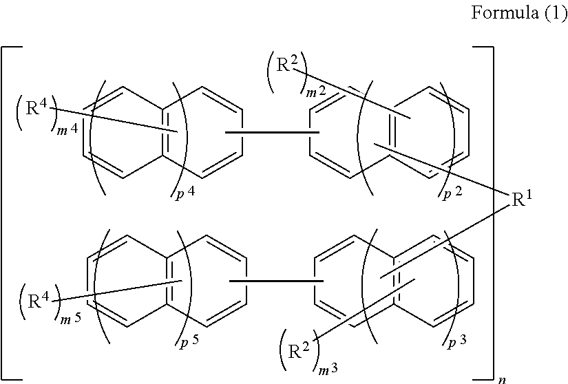
A compound represented by the following formula (1).
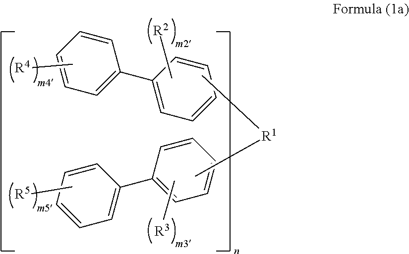
(in formula (1), R1 represents a 2n-valent group having 1 to 30 carbon atoms, R2 to R5 each independently represent an alkyl group having 1 to 10 carbon atoms, an aryl group having 6 to 10 carbon atoms, an alkenyl group having 2 to 10 carbon atoms, an alkoxy group having 1 to 30 carbon atoms, a thiol group or a hydroxyl group, provided that at least one R4 and/or at least one R5 represents an alkoxy group having 1 to 30 carbon atoms, m2 and m3 are each independently an integer of 0 to 8, m4 and m5 are each independently an integer of 0 to 9, provided that m4 and m5 are not 0 at the same time, n is an integer of 1 to 4, and p2 to p5 are each independently an integer of 0 to 2.)

Description

TECHNICAL FIELD[0001]The present invention relates to a compound or a resin having a specified structure. The present invention also relates to a material for forming an underlayer film for lithography containing the compound or the resin, a composition containing the material, an underlayer film for lithography obtained from the composition, and a resist or circuit pattern forming method using the composition. The present invention further relates to a purification method of the compound or the resin.BACKGROUND ART[0002]Semiconductor devices are manufactured through microfabrication by lithography using a photoresist material, but are required to be made finer by a pattern rule in accordance with the increase in integration degree and the increase in speed of LSI in recent years. In lithography using exposure to light, which is currently used as a general-purpose technique, the resolution is now approaching the intrinsic limitation associated with the wavelength of the light source...

Claims


Application Information

Patent Timeline
Patent Type & Authority Applications(United States)
IPC IPC(8): C07C43/275C07C41/38G03F7/11C07C43/235C08G8/10
CPCC07C43/275C07C43/235C08G8/10G03F7/11C07C41/38G03F7/16G03F7/20G03F7/30C07C43/205C08G8/00G03F7/094G03F7/26
Inventor TOIDA, TAKUMIECHIGO, MASATOSHISATO, TAKASHIMAKINOSHIMA, TAKASHI
Owner MITSUBISHI GAS CHEM CO INC
Why Eureka
Try Eureka